0
\$\begingroup\$

I'm having the following problem. I got to analyze a BJT differential pair with emitter degeneration of both transistors. I calculated the theoretical expressions of my gain and obtained (since the transistors are equal):

$$A_{d1}=-\frac{βR_{C}}{2(r_{π1}+(1+β)R_{E} )}$$
$$A_{d2}=\frac{βR_{C}}{2(r_{π1}+(1+β)R_{E} )}$$

The numerical values here don't matter for my question I guess. Then I proceeded to simulate my circuit LTSPICE. As I expected, the values were slightly different from the ones obtained theoretically. What I did not expect was that the values of the gains were slightly different from one another, while that transistor are equal (there should symmetry on the circuit). Why is this happening?

EDIT: Here is the schematic used enter image description here
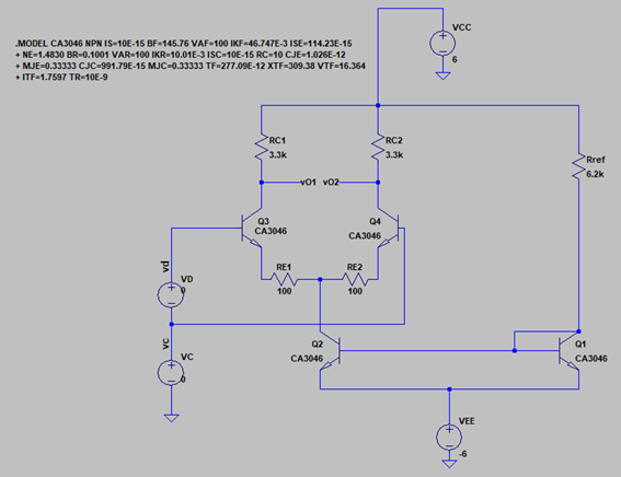
as well as the operating point:

V(n001):     6   voltage
V(vo1):  2.9365  voltage
V(vo2):  2.9365  voltage
V(n003):     -0.746863   voltage
V(n002):     -0.653111   voltage
V(n004):     -0.653111   voltage
V(n005):     -5.32863    voltage
V(n006):     -6  voltage
V(vc):   0   voltage
V(vd):   0   voltage
Ic(Q2):  0.00187503  device_current
Ib(Q2):  1.74223e-005    device_current
Ie(Q2):  -0.00189245     device_current
Ic(Q3):  0.000928333     device_current
Ib(Q3):  9.18252e-006    device_current
Ie(Q3):  -0.000937515    device_current
Ic(Q4):  0.000928333     device_current
Ib(Q4):  9.18252e-006    device_current
Ie(Q4):  -0.000937515    device_current
Ic(Q1):  0.00179235  device_current
Ib(Q1):  1.74223e-005    device_current
Ie(Q1):  -0.00180978     device_current
I(Rref):     0.0018272   device_current
I(Re2):  0.000937515     device_current
I(Re1):  -0.000937515    device_current
I(Rc2):  0.000928333     device_current
I(Rc1):  0.000928333     device_current
I(Vc):   -1.8365e-005    device_current
I(Vd):   -9.18251e-006   device_current
I(Vee):  0.00370223  device_current
I(Vcc):  -0.00368386     device_current

I notice that the current flowing in each of the voltage sources is a little bit different... Could that be the reason? And why are they different?

\$\endgroup\$
16
  • 1
    \$\begingroup\$ Provide a schematic (yes, of course, we all know what a BJT diff-pair, or a long-tailed pair, is.) But I'd rather not assume anything. I'd also like to see your development because that shows me where your questions really lay. You suggest symmetry, but I honestly have no idea how you TESTED this. And I'd like to see how you did. Show me. (You say you did this in LTspice, so it should be easy to include the netlist from it, for example.) \$\endgroup\$
    – jonk
    Commented Jun 3, 2018 at 5:57
  • \$\begingroup\$ Hi! Thanks for the quick answer. I edited the question to provide a little bit more information. \$\endgroup\$ Commented Jun 3, 2018 at 6:16
  • \$\begingroup\$ Which specific numbers are you comparing and finding different. You list all of them. Provide a focus for me. [Sidebar: CA3046 is getting hard to find these days. My favorite the CA3096 (which should have the PNP's improved, damn them) is even harder, I suppose.] \$\endgroup\$
    – jonk
    Commented Jun 3, 2018 at 6:21
  • 1
    \$\begingroup\$ I'm curious about what you're doing there with VC and why you aren't feeding each input of the differential pair with its own ground referenced V_D/2 source? \$\endgroup\$ Commented Jun 3, 2018 at 6:27
  • \$\begingroup\$ @jonk I was comparing I(Vee) and I(Vcc). They are different but should they? \$\endgroup\$ Commented Jun 3, 2018 at 6:40

1 Answer 1

1
\$\begingroup\$

Both gain values can be equal only if two conditions are met:

(1) The circuit is 100% symmetric (fulfilled)

(2) Both signal input voltages (between B and E) are equal (not fulfilled).

For a good understanding of the circuits function it is essential to realize that - for each of the transistors - the voltage Vbe matters (and not only the voltage at the base node).

  • For Q3: Vbe=(Vc+Vd)-Ve =Vc-Ve +Vd

  • For Q4: Vbe=Vc-(Vdx+Ve)=Vc-Ve -Vdx.

(Ve is the DC voltage - equal for both transistors - caused by the common DC current source)

What is Vdx? In contrast to Q3, the transistor Q4 receives an input signal (caused by Vd) from the emitter of Q3 (acting as a emitter follower). This voltage Vdx is slighly smaller than Vd (emitter follower gain <1). The voltage at the base of Q4 is the DC voltage Vc only!

Interpretation (for a correct understanding): Both transistors (Q3 and Q4) can be seen as a series connection of a common-collector and a common-base stage.

Result: Thus, the positive input swing for Q3 (Vd) is not identical to the negative input swing for Q4 (Vdx).

\$\endgroup\$

Your Answer

By clicking “Post Your Answer”, you agree to our terms of service and acknowledge you have read our privacy policy.

Not the answer you're looking for? Browse other questions tagged or ask your own question.