Gh-B, I am afraid, there is a kind of misunderstanding on your side.
- At first, let me quote and comment a sentence from Dan Fritchmans answer:
"Generally for non-linear circuits, this is not a constant number, but a function of input signal"
For my opinion, this can lead to severe misundestandings. Every transistor based amplifier is a non-linear circuit and needs DC biasing. Of course, if the input signal contains a DC voltage the quiescent operating point (and, with it, the transconductance and the gain) will change its value. But this is not the classical case. Normally, we bias such a non-linear device separately and independent on the "input signal" to be amplified. And this also applies to the differenetial amplifier under discussion.
Speaking of an "input signal" we, normally, refer to periodic excursions around a fixed operating point (without any DC portion) - and the transconductance (and the gain) will remain constant - as long as the excursions are within a limited (small) range: Small signal conditions. For a differential amplifier this range is as large as (50---60) milliVolts.
- Your sentence:"...but if the current is steered to one side (ignoring the leakage current ) then gm of that side will be = 1m / 25mv = 40mS then what will the differential gain be ?"
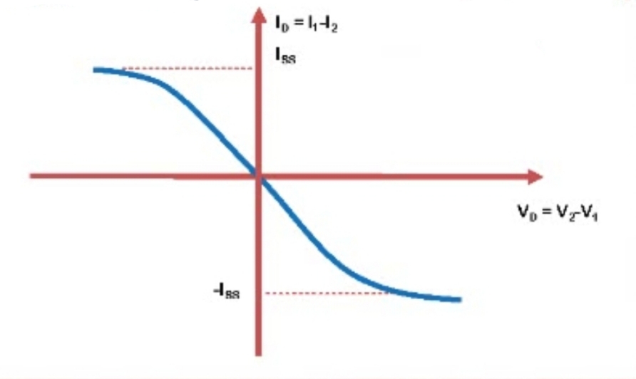
This is an extreme case (one transistor off) and we cannot speak about "signal gain" at all because it is not possible to allow signal excursions in two directions around this point. Of course, we can identify a slope of the transfer curve under these conditions - but for which purpose? It is a pure theoretical number without any practical relevance.
- Therefore: The shown transfer characteristic Id=f(Vd) is a tanh-function and can be used for "linear" (better: quasi-linear) amplification purposes around the midpoint (at Vd=0) for signal values (and a signal consists of Vd variations) within a small range. This range is limited by the allowed non-linearities which are application dependent.
And the transconductance gm is considered as constant and is defined by the slope of the curve at Vd=0.
Example: For input amplitudes of 50 mV the signal distortion (THD) caused by the non-linearity of the tanh-characteristic will be app. THD=5%.
Final comment: Of course, we can imagine a (theoretical) case, where we have a constant input voltage (DC) at one transistor and a "signal voltage" at the other transistor. In this case, the "DC quiescent point" would be not at Vd=0 - and the slope (transconductance) around this new operating point would be somewhat smaller - but for which purpose? Now the allowable range of signal excursions around this bias point is reduced (due to an increased non-linearity). This is a theoretical case without any practical relevance.

