1
\$\begingroup\$

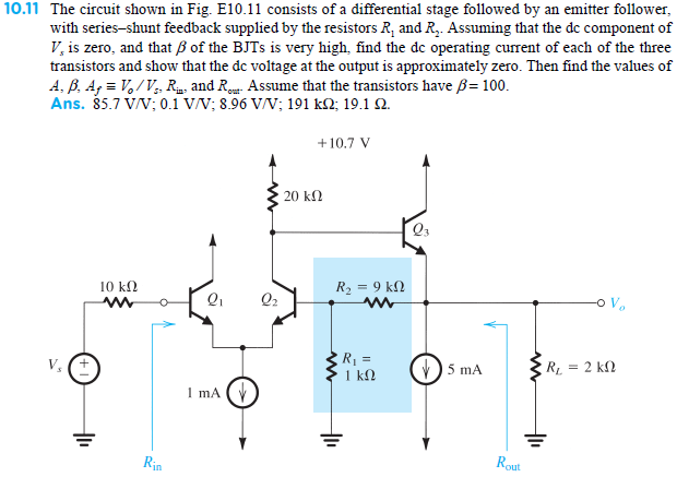
I have an exam next week, and I need to get a real high mark to pass. Therefore I'm looking for some hard questions to solve, and this is one.

enter image description here

While I don't expect a full solution from you here, some guidance would be nice.

  1. What does “assuming B of the BJTs is very high” mean?
  2. How do we seperate the 1 mA source to the differential pair? Because the solution guide says that it is evenly distributed. How?
\$\endgroup\$
2
  • \$\begingroup\$ Hangi hocadan alıyorsun dersi? \$\endgroup\$
    – Alper91
    Commented Dec 27, 2015 at 13:21
  • \$\begingroup\$ Oktay Aytar, AİBÜ \$\endgroup\$
    – C K
    Commented Dec 27, 2015 at 13:30

2 Answers 2

1
\$\begingroup\$

That's not a capital "B", but a beta (β). It refers to the gain of the transistor, collector current divided by base current.

You can consider the 1 mA evenly distributed as a first order approximation. In reality, this only happens right at the cusp where the differential pair is in balance. A little off from that point, and one transistor will rapidly take more of the current than the other.

However, this circuit puts negative feedback around this differential pair, always keeping it close to the balance point. With the input at ground, the other input of the diff pair will also be held close to ground. That requires close to 10 V across the 20 kΩ resistor, which means the right transistor of the pair is drawing ½ mA, so the left one is drawing the other ½ mA.

\$\endgroup\$
4
  • \$\begingroup\$ Thank you for the answer :) I am trying to draw the whole thing as the series shunt topology, but I can't draw the feedforward circuit... The output of feedback circuit should be in series with the signal, but I can't figure out how. Can you help with that? \$\endgroup\$
    – C K
    Commented Dec 27, 2015 at 16:15
  • \$\begingroup\$ @Cetin: I can't make sense of what you are asking. \$\endgroup\$ Commented Dec 27, 2015 at 16:31
  • \$\begingroup\$ I simply ask where the A circuit is according to this picture: images.slideplayer.com/16/4939071/slides/slide_2.jpg \$\endgroup\$
    – C K
    Commented Dec 27, 2015 at 16:47
  • \$\begingroup\$ The gain A is simply the forward gain without any feedback. \$\endgroup\$
    – LvW
    Commented Dec 27, 2015 at 18:27
0
\$\begingroup\$

One key to find the solution is the information about B resp. β, which is allowed to be assumed as very high. This means that you may neglect the base currents. This assumption drastically simplifies the whole calculation. As an example: This assumption simplifies the calculation of the voltage division between R1 and R2. More than that, the base potential for Q1 can be set to zero.

\$\endgroup\$
2
  • \$\begingroup\$ Hmm... so no current flows through base of Q2 either. And we know that base voltage of Q2 is also 0 volts. Therefore no current will flow through R2 too, and Vo becomes 0 volts. Am I correct? \$\endgroup\$
    – C K
    Commented Dec 27, 2015 at 15:18
  • \$\begingroup\$ Yes - as a first approximation (neglecting base currents). this is OK. For calculation of gain values you need the input resistance for Q3. \$\endgroup\$
    – LvW
    Commented Dec 27, 2015 at 16:56

Your Answer

By clicking “Post Your Answer”, you agree to our terms of service and acknowledge you have read our privacy policy.

Not the answer you're looking for? Browse other questions tagged or ask your own question.