1
\$\begingroup\$

Let me start off by saying that this is not homework! I am several years removed from the fun of college.... However, one of my main hobbies is electronics tinkering and I am referring to an intro ECE text from college.

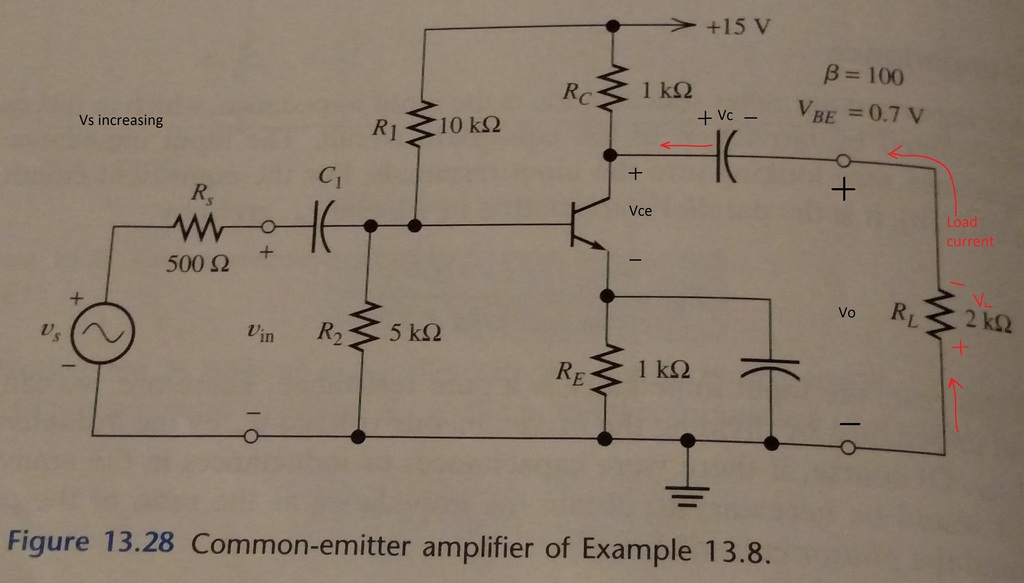
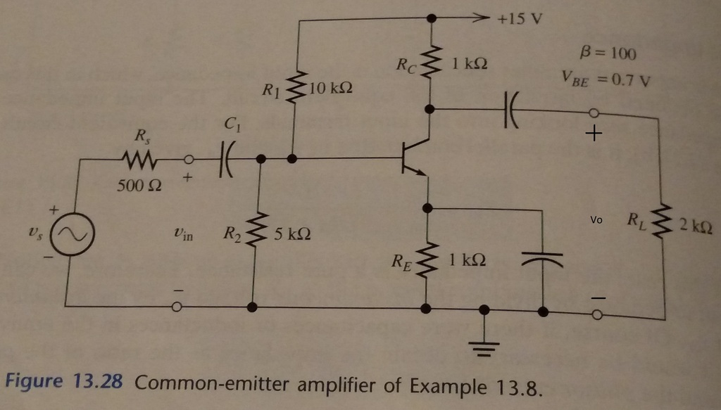
An example problem in my book deals with the common emitter circuit shown below. The DC bias point analysis is straightforward. For the small signal AC analysis, my book teaches a method of approximating the BJT as a resistance and a current controlled current source (not shown). I understand how all the various gains are then found, but I don't understand how the output voltage can go negative.... The output voltage is Vo and it is across the load resistor RL.

enter image description here

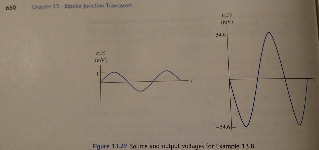
The next figure in my book gives side-by-side graphs of the input signal Vs (given by Vs = 0.001sin(wt) V ) and the output voltage Vo.

enter image description here

I am not seeing how Vo can be negative! I have seen several other common emitter examples and they all seemed to have an output voltage that stayed positive (riding on a DC bias). Also, if you need to know, the calculated voltage gain was Av = -106

A paragraph in the book states that the source voltage Vs divides between the internal source resistance Rs and input impedance Zin of the amplifier. When that calculation is performed, we get that Vo(t) = (Av)Vin = -54.6sin(wt) mV

\$\endgroup\$
2
  • \$\begingroup\$ There's a cap before (in series with) the output/load: the top-right corner one (has no id/label). That removes the DC bias so the load sees only AC. \$\endgroup\$ Commented Sep 30, 2015 at 1:53
  • \$\begingroup\$ @RespawnedFluff Hi thanks for the prompt reply. Can you take a look at my answer below to my own question and see if my reasoning makes sense? \$\endgroup\$ Commented Oct 1, 2015 at 22:25

5 Answers 5

3
\$\begingroup\$

One important component in the circuit is the output capacitor between RC and RL.

At power up it will charge up to the DC voltage present at the collector of the transistor and from then on will act as if it was a battery and keep a constant DC voltage across it.

When the transistor takes more current as a result of the input signal it will cause the voltage at the collector to drop and this will be transferred through the capacitor to the load RL.

Since the assumption is that the capacitor voltage remains constant the voltage at RL will go negative. (below ground)

Similarly if the transistor current reduces the voltage at the collector will go positive and this will be communicated through the capacitor to RL which will then go positive relative to ground.

In order for the voltage across the capacitor to be unvarying the time constant of the capacitor and RL must be much greater than the period of the signal being amplified.

This type of "capacitor coupling" is common in amplifiers where the DC component of a signal is unimportant such as in audio or RF amplifiers.

The capacitors at the input (C1) and on the emitter will also have been selected to be large enough that the voltage across them remains constant for a complete cycle of the signal.

\$\endgroup\$
1
  • \$\begingroup\$ Thanks for this explanation. When I compared to the above circuit to the other common emitter circuits in my book, I wasn't noticing that those circuits did not have the capacitor on the output. Thanks also to the others for explanations in different ways. \$\endgroup\$ Commented Sep 30, 2015 at 23:16
1
\$\begingroup\$

There are two dimensions to this : the practical circuit, and the "small signal analysis" theoretical aspect.

Several good answers cover the practical aspects of the circuit : your understanding is correct that at the collector, the DC bias ensures the signal remains positive, but the output coupling capacitor removes that DC bias at Rl.

However it's also important to understand that "small signal analysis" is a simplification - a white lie or a myth, if you like, to aid understanding aspects of the amplifier's design. In this mythical domain, practical circuit aspects like DC bias can be ignored. Thus there are only deviations from the mean value, and to simplify further, the mean is taken to be 0, so that deviations above it are +ve, deviations below it are -ve.

This holds true (in small signal analysis) whether you measure the output at Rl (where the signal really can go -ve) or at the collector (where in reality it can't).

Take what you can from the small signal analysis : it should let you understand that the gain is negative and how it depends on the resistor values. Don't worry if it shows "negative" values from a single supply; just remember it's a simplification, a framework to help understanding one aspect, not the whole.

\$\endgroup\$
1
\$\begingroup\$

Thanks all for the explanations. Due to reading them, I think I have another way I came to understand how the output voltage can go negative. It involves looking at the direction of the Load current.

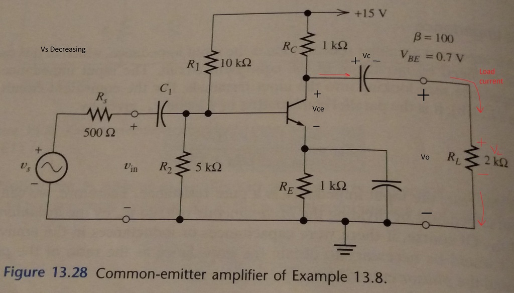
The first image shows the circuit when Vs is increasing. As Vs increases, Vce decreases. Since the output capacitor voltage is basically assumed to be constant, Vce < Vc. Thus this voltage difference causes load current in the direction shown and the resulting sign of the voltage drop across the Load means that Vo will be negative.

enter image description here

In the 2nd image, Vs is decreasing and due to Vce > Vc, the load current is in the other direction causing the load voltage to be positive.

Have I confused myself more or is the above a valid way of understanding this circuit?

enter image description here

\$\endgroup\$
1
  • \$\begingroup\$ Yes, I think this is quite a valid way to think about the circuit. I remember not that long ago I was still working on the mistaken intuition that in a circuit powered by say +15V and 0V (ground), all node voltages in the circuit would be somewhere between those two values. This example shows how that's not always true :) It was about that time I started paying more attention to current flows through a resistor to get a feel for their node voltages rather than the other way around :) \$\endgroup\$
    – scanny
    Commented Oct 2, 2015 at 5:40
1
\$\begingroup\$

I understand how all the various gains are then found, but I don't understand how the output voltage can go negative.... The output voltage is Vo and it is across the load resistor RL.

enter image description here
(source: gsu.edu)

enter image description here

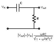
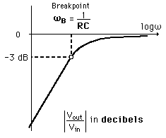
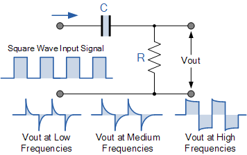
It blocks dc therefore the only content that remains has to be the AC signal that was previously superimposed on a DC level but now cannot be. You can also review its operation as a differentiator: -

enter image description here

Positive going square wave input has to have no DC content at the output therefore the signal level is symmetrical about 0V.

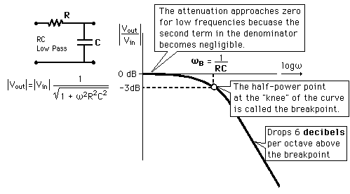
For completeness, here's an RC low pass filter: -

enter image description here

\$\endgroup\$
0
\$\begingroup\$

Quote: For the small signal AC analysis, my book teaches a method of approximating the BJT as a resistance and a current controlled current source (not shown). I understand how all the various gains are then found, but I don't understand how the output voltage can go negative

1) I assume you are referring to one of the classical equivalent small-signal diagrams with an input resistance r,in and a current source ic=ib*beta which is controlled by the current ib through this resistance r,in. As you will notice, both currents (ic and ib) will go into the circuitry. This causes a voltage across the collector resistance Rc which has an opposite direction if compared with the input voltage. This explains the "secret" of the negative sign.

2.) The signal voltage at the output is NOT negative - but it is in anti-phase to the input signal. Hence, considering only this signal voltage (without the DC portion) we can say that the output signal voltage is negative (in comparison to the input voltage). That means: Signal gain is negative because we have a phase inversion between both signals.

3.) This can be explained very easily: The positive half wave of an input signal voltage at the base node causes an increase in collector current. As a consequence, the voltage drop at the collector resistor Rc also increases. Because the positive supply is fixed, the potential at the collector node DECREASES (negative half wave). Hence, we have a signal inversion which is considered in all formulas with a negative sign.

\$\endgroup\$

Your Answer

By clicking “Post Your Answer”, you agree to our terms of service and acknowledge you have read our privacy policy.

Not the answer you're looking for? Browse other questions tagged or ask your own question.