1
\$\begingroup\$

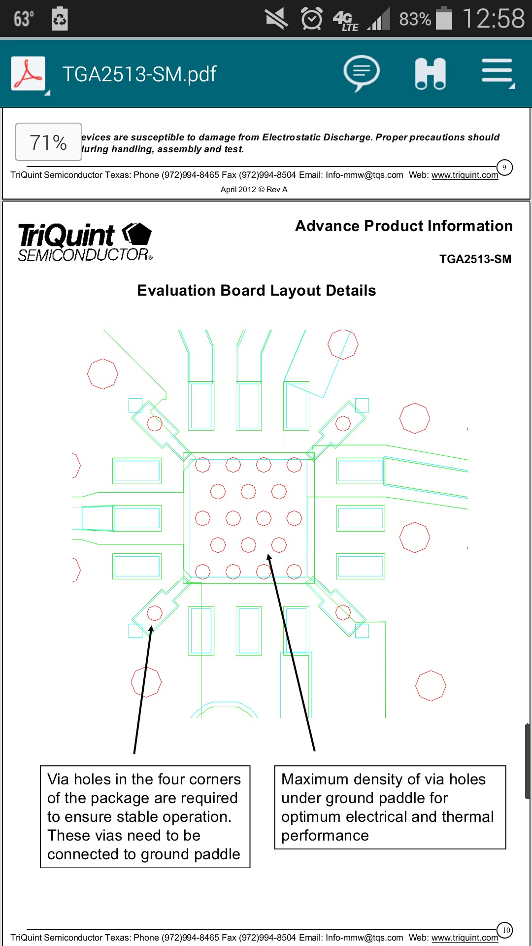
In the picture below, from the recommended layout of the TGA-2513-SM:
picture below

there are via holes in the four corners of the QFN package. The datasheet claims that this "ensures stable operation". In what sense? There are plenty of thermal vias under the pad which also ensures a solid connection to the ground plane. Why are these four corner vias necessary?

The only reason I can think of is these corner pads provide extra heat dissipation. But that doesn't seem like what they meant by "stable operation". This is a wideband LNA by the way.

\$\endgroup\$

1 Answer 1

1
\$\begingroup\$

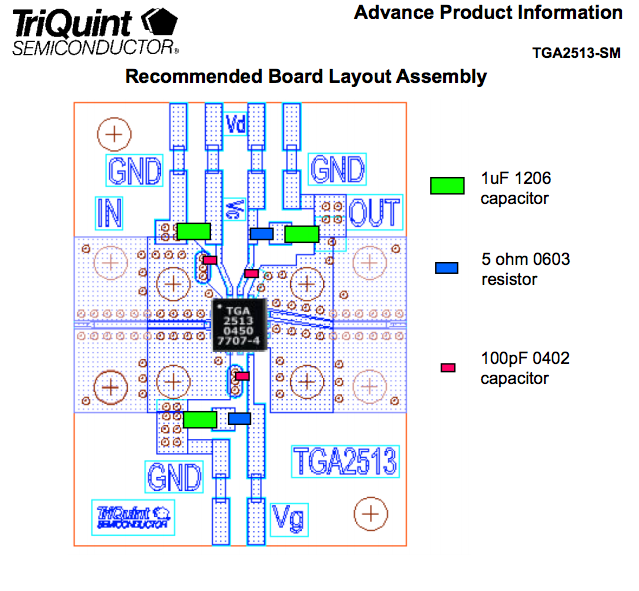
I haven't seen that before, but on the previous page of the datasheet they show an example layout with ground pours coming "out" of those 4 vias. In particular two pours are surrounding the RF in trace and two are surrounding the RF out trace. I imagine the intention is to ensure that the ground surrounding the RF is the same ground as the IC's ground. Looks like this part is meant to operate up to 20 GHz so your ground needs to be super stable/low noise/low impedance path. So I think the goal is that you're directly connecting the pours surrounding the RF in to the GND pad of the IC rather than using vias from the IC to a plane and from the pour to the same plane. Long story short I think they just want you to have a super low impedance return path, which makes a lot of sense especially in the RF world.

enter image description here

\$\endgroup\$
4
  • \$\begingroup\$ That makes sense. They already have some ground pins connected to the ground pours surrounding the rf traces, but none of the ground pins are connected to the ic ground pad. If it were me I would connect the gnd pins to the ic gound pad and not have the awkward corner pads. \$\endgroup\$ Commented Oct 9, 2015 at 17:33
  • \$\begingroup\$ @pikafu That seems like a reasonable alternative and I have to imagine it would work fine. That stated if they're suggesting a certain layout why not just go for it? I've only done a handful of RF heavy boards (and I'm not an "RF guy"), but every time it feels like there's an element of black magic (I'm exaggerating a bit). I'd personally prefer the "brain off" approach and just copy their suggestions so I could sleep well knowing that at least that part of the design should work properly :) \$\endgroup\$
    – Doov
    Commented Oct 9, 2015 at 17:54
  • \$\begingroup\$ Put another way, if you end up having to debug the RF it would suck to have to scratch your head and wonder.."maybe it's the ground connection?" \$\endgroup\$
    – Doov
    Commented Oct 9, 2015 at 17:54
  • \$\begingroup\$ Agreed! I'm just getting into RF layout and there are so many little tips and tricks that can make or break your final board. Copying the recommended layout is the way to go especially in my case where I don't have time to respin the board. \$\endgroup\$ Commented Oct 9, 2015 at 18:53

Your Answer

By clicking “Post Your Answer”, you agree to our terms of service and acknowledge you have read our privacy policy.

Not the answer you're looking for? Browse other questions tagged or ask your own question.