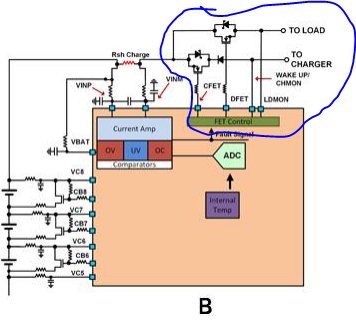
If you take a look at the symbols of each your discrete FETs there, you'll notice they have body diodes present. If you did not have the CFET, and just had the DFET, while you would stop discharging, you would not stop charging if some kind of charger was hooked up because current would flow through the body diode of the DFET. Having both of them solves the problem, and allows you to have operating modes where you discharge only but block charging, and vice versa.
Now, the root of what you are asking I think is, do I use a high-side or low-side battery switch, and this is a loaded question that involves trade off in the amount of circuitry you wish to use.
First, NFETs vs PFETs. There are tons of differences between the two, but the biggest one I would pay attention to here is the on-resistance, or RDS(on) of the transistor. N-channel devices tend to have lower RDS(on) than an equivalent PFET, meaning they will dissipate less power. I would try to use an NFET for this application, and most folks generally do so.
Next, you correctly identified that a NFET is an enhancement-mode device that requires a positive VGS (gate-to-source voltage) to turn on. When used on the low-side, it does not require any additional driver circuitry because it's on the ground return path. When used on the high-side, you need a driver to generate a positive VGS above the source voltage -- generally done with a charge pump.
You can search this site for questions relating to high-side vs. low-side; I don't want to re-type that here as I can't do the answer justice quickly. Here are some considerations though:
High-side NFET
- generally more intuitive to understand (you're removing voltage / power from the system)
- don't have to worry (as much) about sneak return paths that may bypass a low-side switch
- requires more complex drive circuitry (charge-pump, etc.)
Low-side NFET
- "trickier" to understand as most people are not used to the notion of pulling out "ground" from a system
- any stray paths that accidentally bypass this switch can lead to unintentional turn-on of the device (a severe example: a short to the chassis of a device, depending on its grounding scheme, may bypass this switch and any safety it offers)
- simpler drive circuitry (i.e. standard I/O)
As for high-side driver ICs, make sure that you find one that is designed to run at 100% duty cycles. Some high-side driver ICs are designed for switching applications (i.e. power supplies) and can't run 100% without recharging a bootstrap capacitor.
A potential solution is to use those outputs to control the enable pin of a charge pump that doubles the incoming battery voltage -- assuming this fits within the maximum VGS rating of your NFETs, that would do it. Charge pumps are fairly efficient devices, but the addition draw of a charge pump may be more than the additional power dissipation of a P-type device.
I've left out PFETs from this answer intentionally -- yes, you could use a PFET here, but would have to check the following:
- can your battery control IC properly control one? (I.E. can the FET control output pin handle the full battery voltage)
- are you OK with the power dissipation of a PFET and its higher RDS(on)?
- is the overall system efficiency greater with a NFET + charge pump solution vs. a PFET solution?

