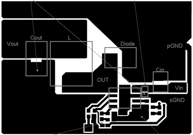
Could you help me understand, why is connecting two polygons of the same net (for example GND) in just one place proposed?
What is difference if we connect pGND (power GND) and sGND (signal GND) with just one track on surface polygon and to make one solid polygon?
They are usualy connected to internal plane through via and they form one net.
Here is an example
1 Answer
By having separate polygons the designer assures currents flow where he wants them to flow. This is not a law, in some cases indeed single solid ground plane may be better. Still, for most cases, it's easier for designer's mind to see where analog/digital/high power currents flow, if they all have separate grounds and are only connected in a single point.
Ah, forgot to mention. The importance of such controlled current flow comes from noises and interference that current may cause. For example, digital currents may create low amplitude high frequency noise in analog circuits. High power currents may cause anything, if they flow under digital/analog circuits. And this is because even ground plane is not ideal, it has resistance, inductance and capacity. Not to mention complex phenomena created by holes in the plane.
By the way, one way is to indeed have separate nets in the design and connect with jumper resistor, and the other way is to call all grounds the same, and cut the polygon in the layout. Then the connection point will have much less resistance and will allow to pass higher currents.
-
\$\begingroup\$ So it is important to connect them in correct spot, when found out where currents should flow. Thank you. \$\endgroup\$– Haris778Commented Feb 17, 2016 at 8:36
-
\$\begingroup\$ Normally the spot will be near the power input. \$\endgroup\$– user76844Commented Feb 17, 2016 at 8:38
