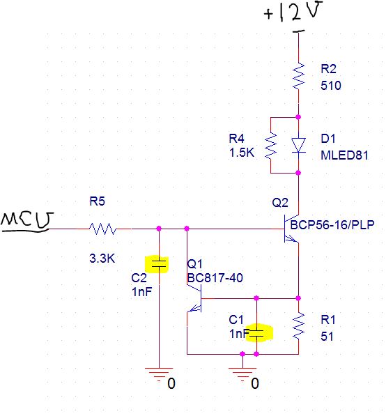
I am trying to analyze a digital circuit. In this circuit, there are several BJT transistors, some for back-light LED driving, some for switching and etc. Almost all of transistor has a 1nF MLCC capacitor connected from base to GND. It seems they are decoupling capacitor, but I am not sure. I really need a reason for this type of design. I asked some people. One of them said this capacitor protects the base of transistor, specially for preventing of unknown switch operating or BCI protecting. (Highlighted capacitors in below picture)

\$\begingroup\$
\$\endgroup\$
14
-
\$\begingroup\$ What's BCI stand for? And a full schematic is required. The context of what's driving the transistor is needed. \$\endgroup\$– PasserbyCommented Oct 2, 2016 at 6:11
-
1\$\begingroup\$ 1nF == .001 uF, not .1 uF \$\endgroup\$– dougCommented Oct 2, 2016 at 6:35
-
\$\begingroup\$ As stated above, a full schematic is required. But note that if you have an input coming from "outside world" then you should place a capacitor to protect that input. Besides, BCI (Bulk Current Injection) test is performed on any input and output coming from/going to "outside world" via a cable and I'm not sure a single capacitor would be sufficient for BCI protection. \$\endgroup\$– Rohat KılıçCommented Oct 2, 2016 at 6:52
-
\$\begingroup\$ Those are fairly odd places for capacitors. Maybe to reduce EMI from PWM? \$\endgroup\$– Ignacio Vazquez-AbramsCommented Oct 2, 2016 at 8:05
-
\$\begingroup\$ @IgnacioVazquez-Abrams Shown LED is drived by MCU(micro-controller) PWM signal. Then, what is your mean from "EMI from PWM"? \$\endgroup\$– ArazCommented Oct 2, 2016 at 8:18
|
Show 9 more comments
1 Answer
\$\begingroup\$
\$\endgroup\$
7
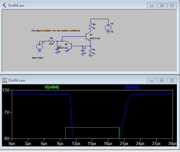
Yes, this is a circuit to limit BOTH edges on a relatively high voltage (12V) signal controlled by (presumably) PWM output from MCU. This is a quick LTspice simulation of the circuit:
Edges are reduced to about 1us rise and fall time. Funny part is that removing of C1 or increasing it to 1uF has no effect on any edge, it is fully defined by C2.
-
\$\begingroup\$ "it is fully defined by C2" -- not surprisingly, since the command pulse must first pass through R4-C2, C1 being only for protection. Actually this is what doesn't make much sense to me: the protection should act immediately, not delayed, so C1 shouldn't be there, but maybe there's a hidden purpouse that I don't see. \$\endgroup\$ Commented Oct 3, 2016 at 7:39
-
\$\begingroup\$ @aconcernedcitizen What you purpose for immediate protection here? TVS or VDR is a expensive solution for this situation. \$\endgroup\$– ArazCommented Oct 3, 2016 at 9:25
-
\$\begingroup\$ Actually, the OP's question (in first edition) was specifically about the purpose of C1. \$\endgroup\$ Commented Oct 3, 2016 at 14:34
-
\$\begingroup\$ @AliChen Would you give me its URL address please? \$\endgroup\$– ArazCommented Oct 3, 2016 at 15:22
-
\$\begingroup\$ Do you mean the free LTspice tool? ltspice.linear-tech.com/software/LTspiceXVII.exe \$\endgroup\$ Commented Oct 3, 2016 at 16:46

