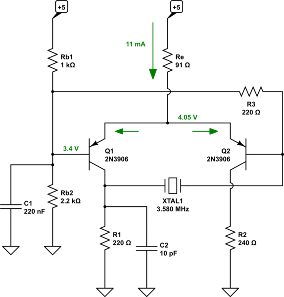
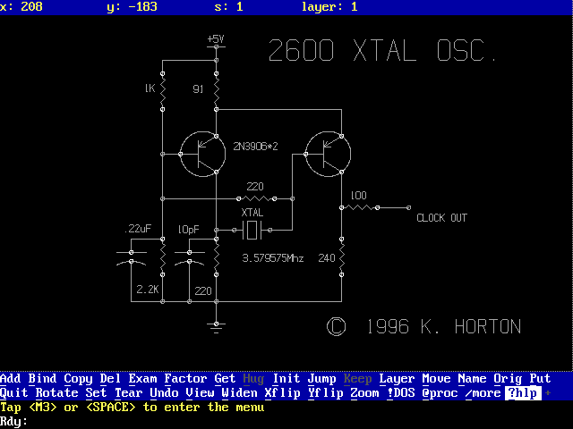
It may be easier to understand if you just start with a long tailed pair -- a differential amplifier. Let me lay it out that way to see if that helps:

simulate this circuit – Schematic created using CircuitLab
I've shown a current and a few voltage values on the schematic. These are roughly true once it starts running. But \$C_1\$ starts out discharged, so those values take a while to reach. At first, \$C_1\$ pulls hard on \$Q_1\$'s base and saturates it, adding current from \$R_e\$ to current from \$R_{b1}\$, in order to charge up \$C_1\$. At some point in this process, and I would guess that it would take about \$\Delta t= \frac{\Delta V\cdot I}{C_1}=\frac{3.4\:\textrm{V}\cdot 15\:\textrm{mA}}{220\:\textrm{nF}}\approx 50\:\mu\textrm{s}\$ before things started rolling, \$Q_1\$ will come out of saturation and things will start to operate more normally. (There's also some diffusion charge storage that was built up into \$Q_1\$, but that's probably only another few added \$\mu\$s. Nothing big.)
As \$Q_1\$ comes out of this initial saturation, it's \$\beta\$ starts to take hold, its base ceases to contribute to charging \$C_1\$, and the voltage drop across \$R_1\$ declines by at least a few tenths of a volt as \$Q_1\$'s \$V_{CE}\$ finally exceeds \$1\:\textrm{V}\$. This drop is passed through the crystal and appears as a slight pull-down at the base of \$Q_2\$, which diverts current through its collector and away from the collector of \$Q_1\$, which causes the drop across \$R_1\$ to decline still further and helps to emphasize this diversion for a moment. However, \$R_3\$ rapidly charges the crystal back up and drives \$Q_2\$'s base back upwards causing it to divert less and allowing \$Q_1\$ to begin diverting more current through its collector, causing the drop across \$R_1\$ to increase again and drive \$Q_2\$'s base further up, as well.
(\$R_{b1}\$ and \$R_{b2}\$ form a Thevenin resistance of about \$680\:\Omega\$. I seem to recall these crystals were about \$100\:\textrm{pF}\$ or so, so working around the loop I see \$680\:\Omega+220\:\Omega+220\:\Omega\$ in series with about \$100\:\textrm{pF}\$ giving about \$110\:\textrm{ns}\$ per half-cycle, which works out to about \$4.5\:\textrm{MHz}\$. So I must be a little wrong about the capacitance of these crystals, I think. The idea is that the natural frequency should be close to the crystal and that the crystal would then "pull it in" tightly.)
Once equilibrium is reached, \$Q_1\$'s base will be very tightly held to its nominal value by \$C_1\$. I think \$C_1\$ is mostly there to hold the base voltage pretty solid and, perhaps indirectly I suppose, to set the start-up timing. It probably could be larger still, with the price being that it would take longer to start up. Most of the variation is taking place at \$Q_2\$'s base. Remember that the collector current will vary by a factor of 10 for a \$60\:\textrm{mV}\$ change in \$V_{BE}\$. \$Q_2\$ will be entirely turned off when its base reaches the \$4.05\:\textrm{V}\$ of its emitter. So I expect that to be the highest voltage seen at the base of \$Q_2\$. The lowest voltage there will be approximately that much, less the voltage drop of \$R_1\$ caused by half the current through \$R_e\$, so I think about \$1.2\:\textrm{V}\$ less, or \$2.85\:\textrm{V}\$ at a guess. In short, I expect \$V_{PP}=1.2\:\textrm{V}\$ at \$Q_2\$'s base, centered relatively close to the \$3.4\:\textrm{V}\$ experienced at \$Q_1\$'s base (with perhaps a very tiny relative offset to it.)
I don't think it would work with either \$R_1\$ or \$R_2\$ changed. Much larger would force the BJT collectors back up against their bases and it wouldn't oscillate. That's one reason they are where they are at. And so you'd have to change \$R_e\$, if you changed them. Also, this would change the natural frequency to be too far away from the crystal and it would oscillate at some other frequency or just fail, even if you changed all three values. So all the pieces seem about right as they are, to me.


