5
\$\begingroup\$

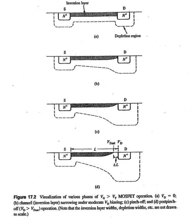
I do understand why when drain voltage (\$V_D\$) increases, the channel carriers decrease (the channel narrows), specially near the drain island, eventually reaching pinch-off phase.

What I don't get is why the depletion region is supposed to widen, as (\$V_D\$) increases.

enter image description here

\$\endgroup\$

2 Answers 2

3
\$\begingroup\$

The schematic shown in question corresponds to an N-channel-MOSFET. The substrate (or body or bulk) of which will be a P-type semiconductor. So source and drain, which are N+ semiconductor regions will form PN junctions with the substrate. The depletion region width of a PN junction increases as reverse bias voltage is increased. Since the voltage applied at drain is positive, the junction becomes reverse biased and hence the width increases with \$V_D\$.

The source and substrate terminals are shorted together to the same potential, that is why depletion width at the source side remains the same while that at the drain side is increasing with drain voltage.

\$\endgroup\$
0
\$\begingroup\$

In addition to the previous answer, a simple way to understand why the depletion region widens is that the increasing positive voltage on the drain will repel more free holes (positive charge carriers) in the p-type substrate that are close to the drain. Therefore leaving behind a larger region depleted of free charges (hence the name). Note that the depletion region is also present in the N+ doped drain but it is much more narrow that the depletion region in the substrate because the drain doping is much higher than the substrate.

\$\endgroup\$

Your Answer

By clicking “Post Your Answer”, you agree to our terms of service and acknowledge you have read our privacy policy.

Not the answer you're looking for? Browse other questions tagged or ask your own question.