I think you're confused with the behavior of a Bipolar transistor.
For a BJT the Collector Base junction will be nearing forward bias to enter saturation mode.
Take note:
for a BJT, saturation means that the transistor does NOT determine the collector current Ic. This happens when \$V_{ce} < V_{ce,sat}\$
for a MOSFET, saturation means that the transistor DOES determine the drain current Id. This happens when \$V_{ds} > V_{ds,sat}\$
we need a reverse bias at Vgs to attract minority carriers from substrate to form a channel No that's not how the channel is formed.
Reverse bias means that there must be a PN junction, there is no junction involved for the gate. The gate is formed when (for an NMOS) the gate potential is higher than the substrate potential + Vthreshold. The positive voltage pulls the negative carriers (electrons) towards the gate oxide to form a channel.

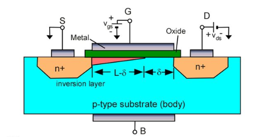
This picture shows the situation when an NMOS is in saturation mode. Note how there is a gap (of length \$\delta\$) between the right end of the channel and the drain. The amount of current that can flow is determined by the shape of the channel, as long as \$V_{gs}\$ remains constant and there is at least some distance between the channel and the drain (\$\delta > 0\$) then the NMOS will remain in saturation.
Channel width and other parameters are indeed all related to saturation mode. It goes a bit too far to explain all the relations here. My advise to you is to think about what happens to the channel in the MOSFET when one parameter is changed like, an increase in \$V_{gs}\$ or a slightly longer transistor.

