0
\$\begingroup\$

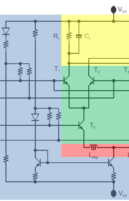
The following picture shows a part of a Gilber-Cell. The yellow part is a low-pass. The green one the mixer core and the blue one determines the operating point of the transistors.

Actually, my problem is to understand the setup for the operating point. Lets assume a Vcc of 5V and a voltage drop across RL of 0.4V. Then we have a collector node voltage at T1 of 4.6V. Now, the operating point has to be determined via the blue network consisting of base voltage dividers: and here I don't get everything.

What I think: The first diode causes a voltage drop of lets say 0.7V. Then I have a voltage divider. What base node voltage do I have to set up? Obviously it must be smaller than the collector node voltage. So, it must be smaller than 4.6V. My Question: How much smaller do I need to set up the base node voltage? Is it just necessary that it is smaller than the collector node voltage or must it be -0.7, so the opposite of Ube?

enter image description here

\$\endgroup\$
9
  • \$\begingroup\$ Look at the schematic, imagine what happens if the voltage at that DC-biasing point (base of T1, T2) is too low or too high. What happens then? If you make the voltage very high that would limit the possible voltage swing at the output (collectors of T1, T2). If the voltage is too low what will happen to T5? The resistors in the blue part of the schematic are chosen such that there is a good compromise between these effects. \$\endgroup\$ Commented Oct 2, 2017 at 8:51
  • \$\begingroup\$ Well, I have to bias T5 independently from T1, right? What I have to check is: if the base node Voltage of T1 is for example 4V, we have a collector node voltage at T5 of ~4V-0.7V=3.3V. Therefore I need to set up the base node voltage of T5 to a value lower than 3.3 V: But how much lower? \$\endgroup\$
    – Max
    Commented Oct 2, 2017 at 8:57
  • \$\begingroup\$ You now base your reasoning on an assumption that VB,T1 = 4V. You can do that but it might not give an optimum solution. For T5 you have to the same as for T1,T2, so what happens when VB,T5 is too low/high, what would be a good choice for T5? Then when you know that, go up to T1,T2. Note that the base voltage and emitter voltage for a transistor are linked (Vbe = 0.7V) but the collector voltage is not, it is determined "from above". \$\endgroup\$ Commented Oct 2, 2017 at 9:03
  • \$\begingroup\$ Ok, back: Collector node voltage of T1 is 4.6V. My problem is that I dont know what base node voltage I have to set up for T1. It must be definitely smaller than 4.6V but it shouldn't be to small, as it determines Uce=Ucb+Ube. So, if it is to small, Uce is to high and there is to much current. If the base node voltage is to high, the transistor will change its mode to saturation? But what will be the optimum node Voltage for T1,T5, respectively? Is it 0.7V below the collector node voltage? \$\endgroup\$
    – Max
    Commented Oct 2, 2017 at 9:14
  • 1
    \$\begingroup\$ @BrianDrummond The popular NE602 Gilbert Cell runs with +6V Vcc. Like the OP's scenario, its top collectors are biased only 0.6v below Vcc. Not much headroom, and its IP3 sucks, because its internal biasing is meant for low-current use. \$\endgroup\$
    – glen_geek
    Commented Oct 2, 2017 at 14:46

1 Answer 1

1
\$\begingroup\$

Look at two DC biasing extremes. One starts from Vcc and works down, the other starts from Vee and works up.

Working from the top down:
If voltage drop across RL is set at 0.4V, then peak AC voltage (max) would be 0.4V as well, setting peak-to-peak voltage at 0.8V. In that case, base voltage of T1, T2 should be no higher than Vcc - 0.8V. You might want a little more headroom to stay out of saturation region, so base voltage T1,T2 should be no higher than 4.0V above Vee. This sets T1, T2 emitter at 3.4V above Vee.
T5's base (to stay away from saturation) should be no higher than 3.2V. T5's emitter would then be 2.6V.


Working from the bottom up:
Leave a generous 0.6v for the current source bias resistor (which could be as low as zero ohms). This leaves lots of headroom for the current source biasing at the bottom transistor. This is an arbitrary decision. Current source Vbe is 0.7V, and again, to stay out of saturation, current source collector voltage adds 0.2V, putting collector at 1.5V above Vee.
T5's base adds 0.7, and should be biased no lower than 2.2V. T5's collector (to avoid saturation) should be no lower than 2.4V.
T1&T2's base adds 0.7V to 2.4V, and should be biased no lower than 3.1V.


These two biasing scenarios define a biasing window for T1&T2, and for T5. T1&T2 bases could sit anywhere between 3.1 - 4.0V. If biased at 3.1V, little headroom is left for T5. It might be wise to split the headroom evenly, and bias T1&T2 bases mid-way in the window at 3.55V.

\$\endgroup\$

Your Answer

By clicking “Post Your Answer”, you agree to our terms of service and acknowledge you have read our privacy policy.

Not the answer you're looking for? Browse other questions tagged or ask your own question.