0
\$\begingroup\$

I've got a doozy of an Altium question:

I've got a chip antenna (2mm x 2mm or something like that).

The datasheet of the chip antenna calls for a 50 ohm line (in red in the graphic)Chip Antenna
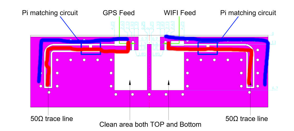
It also calls for a GND line (in blue) that intersects the 50 ohm trace.

Supposing I draw this layout in Solidworks and import it as a top layer fill, so the geometry of the traces are correct?

How would you assign the nets and/or layout the pads to the top layer fill of this shape?

I've tried creating the separate fill and it seems you can't assign just a chunk of the top layer fill to a net.

In this post showing a kind of similiar issue, what did the user do here to create those pad points? Did he just create a top layer pad and drop it on the fill?

This is like a pro-grade Altium problem.

\$\endgroup\$
7
  • \$\begingroup\$ The best I have got working is to import a DWG from Solidworks. The DWG is of the antenna geometry. And than drop seperate pads at each feed point on the antenna ( so there are five pads in total, on the left a GND & 50 ohm signal, center 1 GND, on the right GND & 50 ohm signal). Is there a better way to do this? \$\endgroup\$
    – Leroy105
    Commented Oct 18, 2017 at 19:49
  • \$\begingroup\$ Google "Net Tie" in the altium documentation. \$\endgroup\$
    – The Photon
    Commented Oct 18, 2017 at 20:35
  • \$\begingroup\$ Google "shoot myself in the face" while reading the Altium documentation. I did end up using a "net tie" in spite of the documentation. I know everyone gets snarky about "reading the datasheet" -- but Altium documentation is the worst, it is all "what" never a "how". You create a top layer fill of the geometry, create pads for each feed point. If you enable "net tie" in the SchLib settings of your components, when you export it to the PcbDoc you can tie multiple nets to the top layer fill you've created. \$\endgroup\$
    – Leroy105
    Commented Oct 18, 2017 at 20:44
  • \$\begingroup\$ The top fill however is not what I need, because it needs to be a trace... I'm guessing you want the pads from the geometry in and then, the traces you draw in Altium... \$\endgroup\$
    – Leroy105
    Commented Oct 18, 2017 at 20:50
  • \$\begingroup\$ You can make the whole antenna a "net tie" footprint. Designate one portion of it a pad to connect to the ground net, and one portion of it a pad to connect to the feed net. Now connect to those pads however you like, with traces, with polygons, or with regions/fills. \$\endgroup\$
    – The Photon
    Commented Oct 18, 2017 at 20:52

1 Answer 1

1
\$\begingroup\$

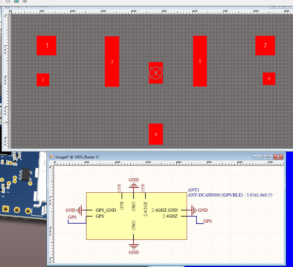
The way I solved this was creating a DWG of the traces I wanted. I then created pads that represent the feed points.

(Just imagine that 6 is the GPS feed, 7 is the GPS GND feed, and 5 is where both of the signals meet.) 1,2,3 are the Wifi feed. Pads 4 and 4 are the ANT GND.

Originally, I thought I would use the top layer fill, but that ends up creating a PCB trace antenna. The signals actually need to be traces that end up at pads.

You can see in the schematic symbol, that I created the ANT GND by using two pads. I think I probably will just make it one.

For the traces, I'll probably connect them using a polygon. Unfortunately, you can't define a net using the fills, which is why I am just left with pads.enter image description here

If you select "net tie" when you create the schematic symbol, Altium will let you "short" (ie. you can merge the nets) in the PCB editor.

\$\endgroup\$
3
  • \$\begingroup\$ The nets on the right hand side that are "GPS" that go to 2.4GHz, should be the 2.4 GHz nets.... But you get the idea... \$\endgroup\$
    – Leroy105
    Commented Oct 18, 2017 at 21:50
  • \$\begingroup\$ ALSO -- I could only get this to work using fills and associate them with the, polygons didn't connect to different nets... Maybe there is way to do it, I couldn't figure it out. A fill is sufficient. \$\endgroup\$
    – Leroy105
    Commented Oct 18, 2017 at 22:21
  • \$\begingroup\$ ALSO -- Tent the tops of the feed pads, but leave the mounting pads exposed. TALK ABOUT CONFUSING. \$\endgroup\$
    – Leroy105
    Commented Oct 18, 2017 at 22:38

Your Answer

By clicking “Post Your Answer”, you agree to our terms of service and acknowledge you have read our privacy policy.

Not the answer you're looking for? Browse other questions tagged or ask your own question.