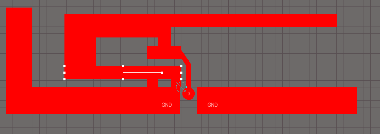
I'm designing a reverse F antenna. It is connected to ground and the antenna line.
It is built of several place fill with small overlaps. To do this, I declared the component as a net tie. The package exposes 2 ground pads and one antenna pad (called 0 on the pictures).
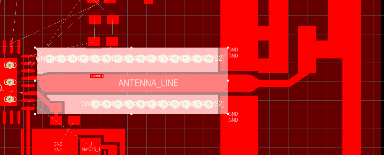
Now I'm facing an issue while placing it on the pcb :
I designed a ground plane around the antenna line and set the clearance rule for this net in order to get the correct impedance.
Problems :
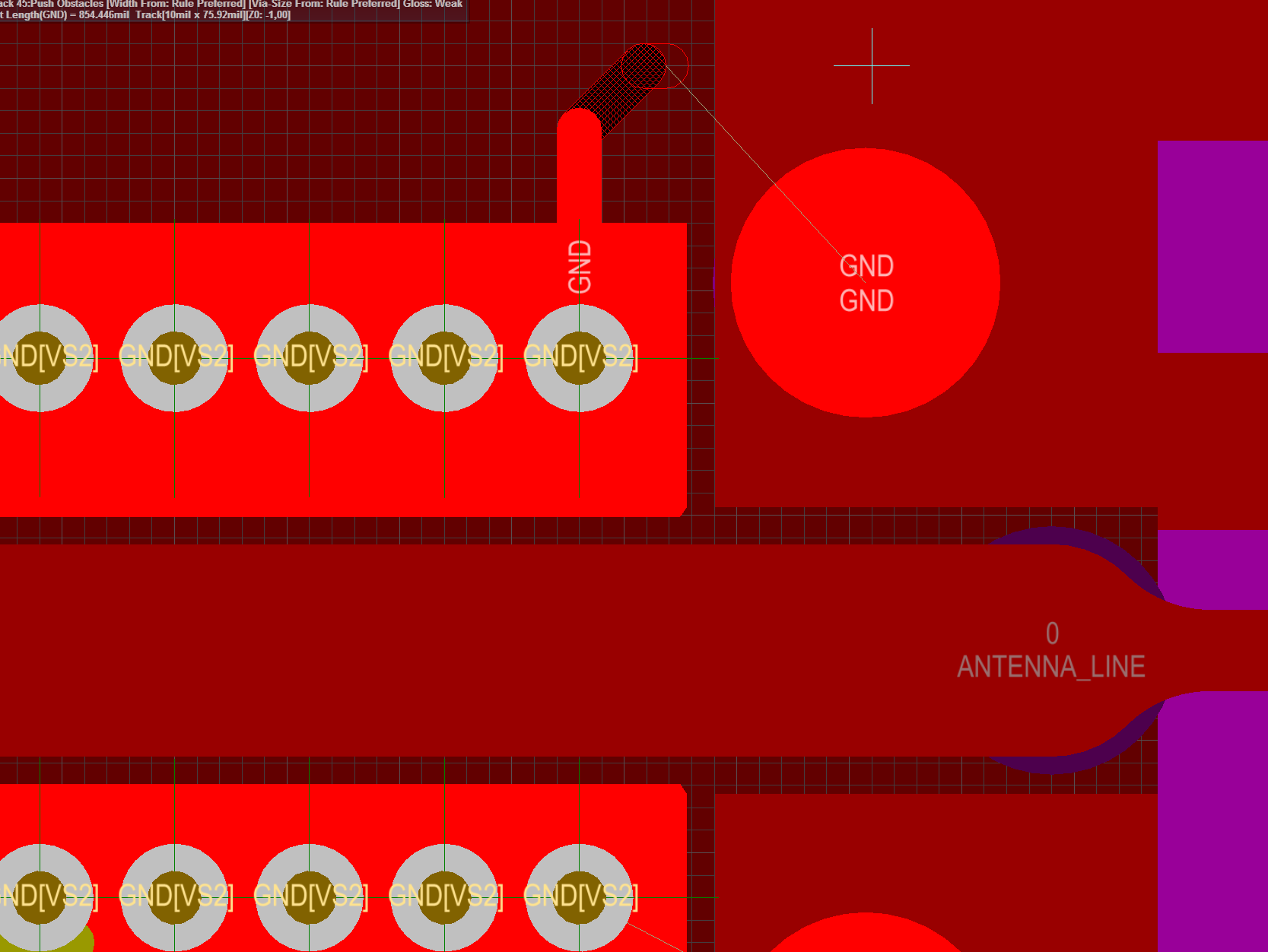
- The ground plane is poured against the ground plane of the antenna.
- I tried to connect the ground plane and the ground pins of the antenna but I'm not allowed to do this. I suspect that altium assumes that there the whole antenna is connected to antenna line and therefore does not allow to reach the ground pad.
Do you have any idea on how to solve this issue ?


