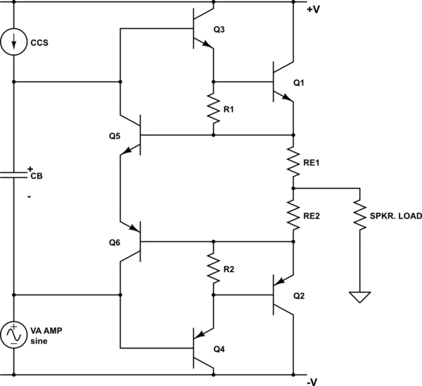
In my book there is a circuit like the one shown bellow. The author (G. Randy Slone) explains the operation and performance of it but there is still one thing that left me wondering.

simulate this circuit – Schematic created using CircuitLab
- Since the signal from Voltage Amplification (VA) stage is not applied directly to both of bases of Q3 and Q4 but only for Q4, how can whole sine wave be normally buffered through the Output Power Stage (OPS)? Or does the signal from the VA goes to both of the bases via capacitor? Since author wrote: "...CB filters small signal variation applied to bias network...", does that mean that VA signal goes to the base of Q3 via CB?
