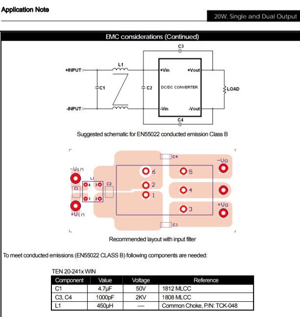
As part of my circuit, I need to step down voltage from +15V to +-12V. For this purpose, I am using Traco TEN 20-2422WIN. I was going through its application note when I saw that they because of EMI, advice to connectC3 and C4 between input and output. Can anyone elaborate on possible reasons for this 
-
4\$\begingroup\$ EMI == black magic \$\endgroup\$– SelvekCommented Sep 28, 2018 at 22:26
-
\$\begingroup\$ @Selvek Care to decode the magic tricks? \$\endgroup\$– AutobotCommented Sep 28, 2018 at 22:31
-
1\$\begingroup\$ Ha every time I get embroiled in something EMI-related at work, I do my best to shift myself on to literally any other project :) My advice? Copy the application circuit and don't worry too much about it! \$\endgroup\$– SelvekCommented Sep 28, 2018 at 22:43
2 Answers
C3,4 1000pF is much smaller Z than the input and output Z yet lower ESR. It it is a form of differential input and output negative feedback to lower the output impedance with rising frequency within driver's bandwidth that works for this unit. So it affects some f>>1/RC for abrupt load changes.
Pulsed high current loads can lead to transients on both output and input. Most often these transients cause interference on the sensor cables due to common mode unbalanced impedance in micro or milliohms between Vout and Ground frame.
The input you show for AC is called a "Line Filter" and for DC often called a BALUN to balance unbalanced differential power or signals by raising the series impedance and cross-winding connections to then cancel so the differential impedance is low but Zcm is high thus less stray EMI current to nearby inputs or cables.
The output cap must follow the OEM's recommendation and is often distributed to each load with single or multiple parts to stored surge energy and thus reduce stray current loops and voltage spikes.
By the way, your converter boosts voltage on the output to 24V split (dual 12) outputs, so current must be increased on the input to consume the same power (V*I) plus losses.
More detailed answers may be researched on PSU EMC or EMI reduction for power supplies for electromagnetic compatibility. (EMC)
-
\$\begingroup\$ Regarding the 'step down ', my mistake. Regarding your answer, I understood the first two paragraphs but not the one regarding the output cap, but I'll do more reading in detail as you advised \$\endgroup\$– AutobotCommented Sep 28, 2018 at 22:49
-
1\$\begingroup\$ if a step load is I then dV/dt=Ic/C is the slew rate of the voltage spike and this <10us transient is best buffered by additional output caps as required with ultra low ESR. Each application can differ, so OEM Application Notes is best start. \$\endgroup\$– D.A.S.Commented Sep 28, 2018 at 22:52
-
1\$\begingroup\$ If your load is more or less constant then it is not always needed but may help reduce ripple noise to desired levels. e.g. 270 µF max with xx mOhm ESR \$\endgroup\$– D.A.S.Commented Sep 28, 2018 at 22:55
-
\$\begingroup\$ I understood your point but can't the purpose of delivery energy during load transient (and limiting dv/dt) be also served with a low ESR cap between +- Vout and com? Why connect between Vin and Vout. Is it because of the ability to store higher energy in those caps due to more voltage difference between output and input (and hence can be done with a smaller cap). Let me know if I have got it all wrong \$\endgroup\$– AutobotCommented Sep 28, 2018 at 23:09
-
2\$\begingroup\$ 1000pF is much smaller than the loads, but it is a form of negative feedback to lower the output impedance with rising frequency within driver's bandwidth that works for this unit. So it affects some f>>1/RC for abrupt load changes \$\endgroup\$– D.A.S.Commented Sep 28, 2018 at 23:13
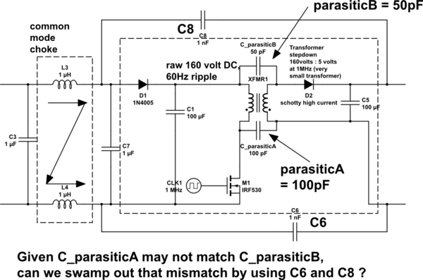
This is how I'm envisioning those two OUT_IN capacitors C6 and C8:

simulate this circuit – Schematic created using CircuitLab
