0
\$\begingroup\$

I have this MOSFET Driver IC 16 Pin Package

Specification - Maximum Drain Voltage 16V. Maximum Drain Current 7.5A

EDIT:

Schematic : enter image description here All the Enable, Sen and Sel signals will be provided by a separate MCU. MCU Datasheet But the below tests are done by isolating the Microcontroller section and giving the signals separately from a power supply and monitoring the output behaviour at the load and the output at the multisense pin.
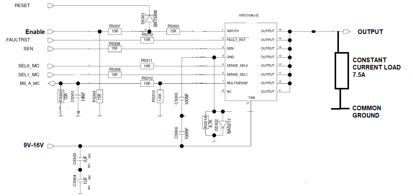
I am giving an external 5V Input to the MOSFET Gate (at pin 1) from this 30V 3A/6A Power Supply - Power Supply Datasheet

So, I am giving 5V to the gate from the power supply and 16V to the drain of the MOSFET (TAB = Vcc) from another similar power supply. I Connected a load of 7.5A between the output pins of the IC (pins 9 -16) to ground. (Electronic Load Used - Constant Current)

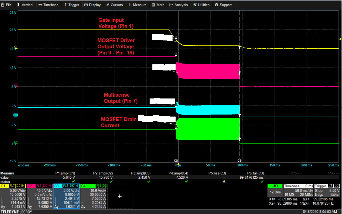
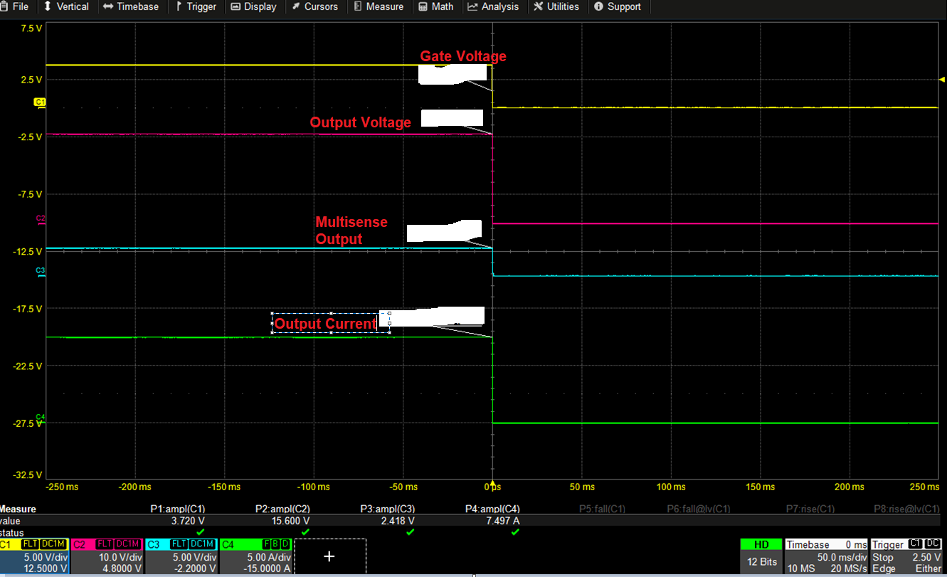
I turn ON and turn OFF the gate voltage to the MOSFET. But When I turn off the 5V input to the MOSFET, I am getting voltages like this (Observing strange switching behaviour during falling):

If Drain Voltage Vcc = 16V

enter image description here

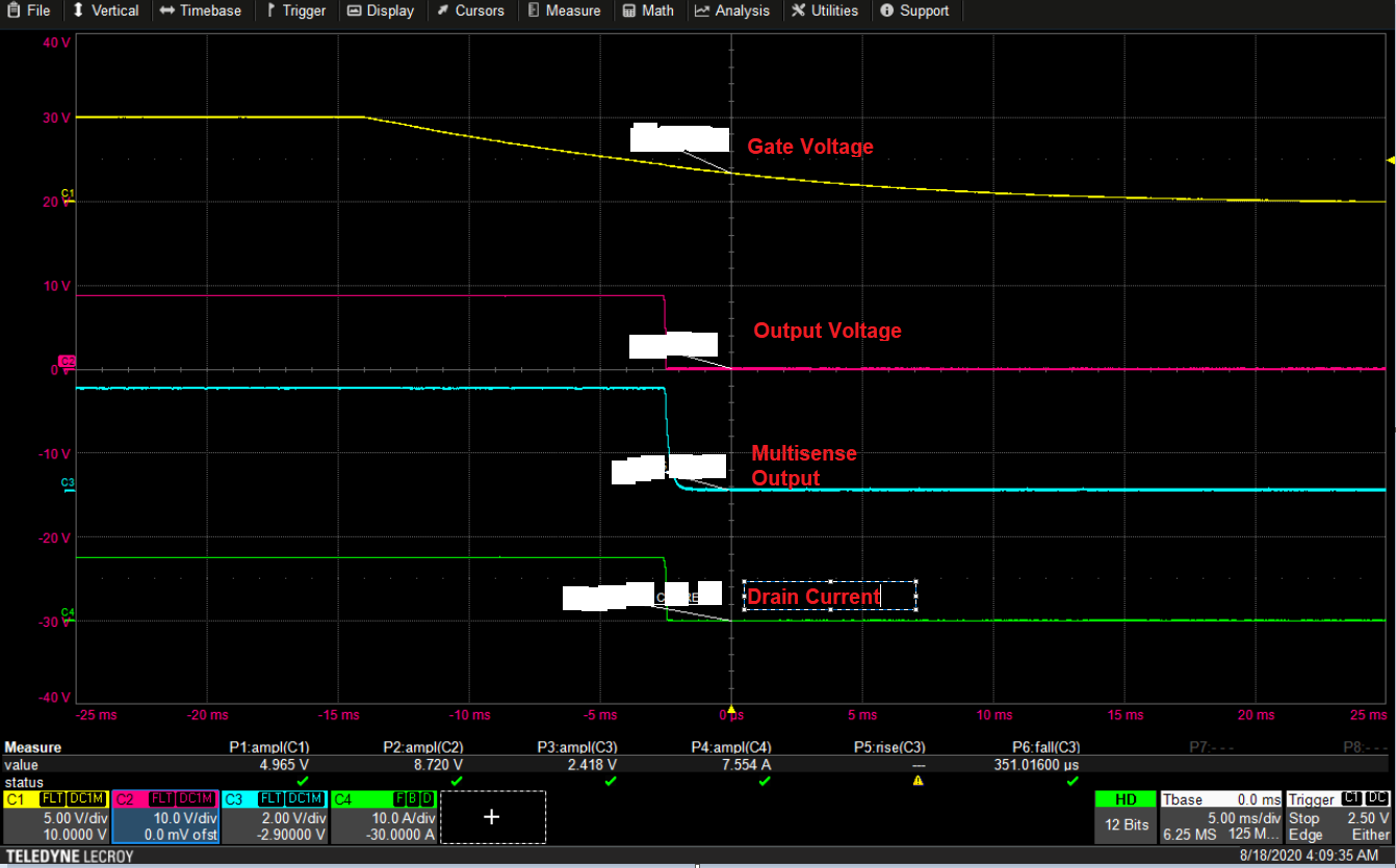
However, If I reduce the drain voltage to Vcc = 9V

The I get this,

enter image description here

I am not able to understand why this behaviour is occuring when I give High Vcc to the IC.

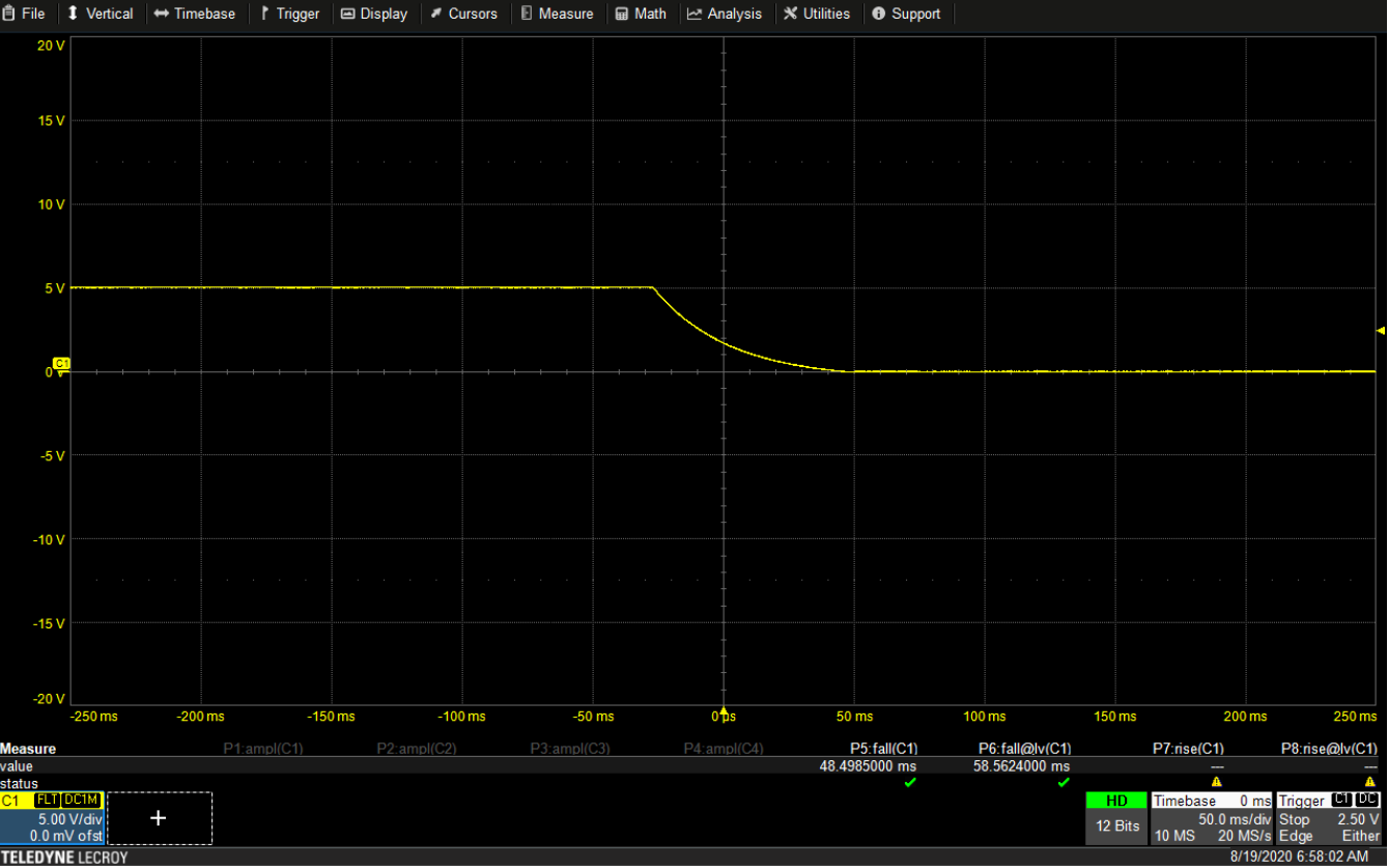
Then, to check the fall time of the power supply (the channel which was connected to the enable gate of the IC)

Fall time was very high. Like in the order of 50ms.

enter image description here

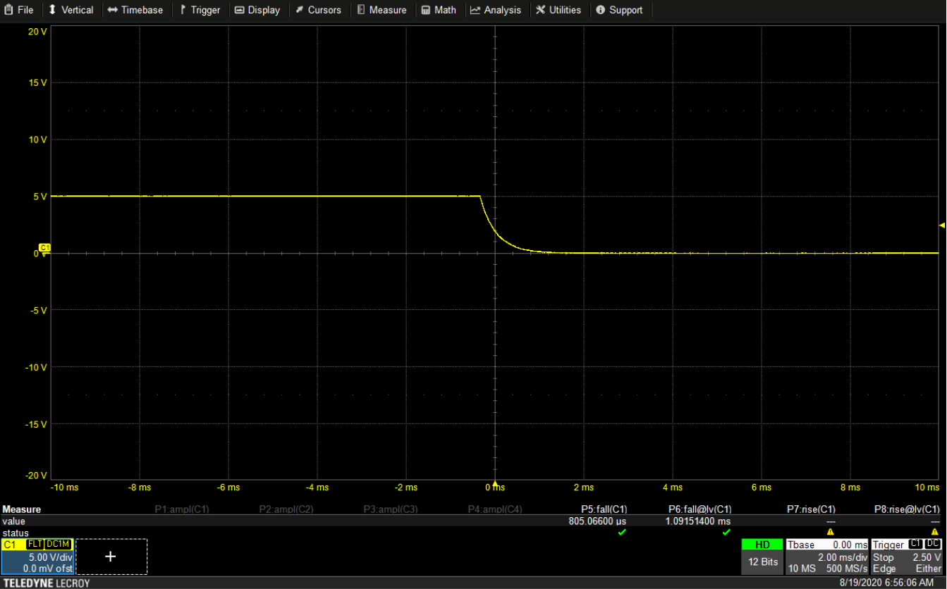
Then, I gave the Input to the gate of the IC using AFG1062 a function generator.

I checked the fall time of the FG. It was around 1ms.

enter image description here

So, now I gave the gate input using the FG itself and set the drain voltage Vcc to 16V using another power supply.

Now, I am not getting the strange switching behaviour during the gate disable time.

enter image description here

My questions :

  1. Why did I get that strange switching behaviour during the fall duration when I used the Power Supply instead of FG? I figured that I could solve the problem if I provide low fall times to the gate input of the IC. But what is happening if I give a fall time so high in the order of 50ms? I tried to look up the fall time or the voltage droop parameter in the power supply manual, but I could not find it. Can someone explain me why this is happening and how to understand this behaviour? What should I look for over here?

  2. Why that strange behaviour was occuring only at Vcc = 16V and not when Vcc = 9V?

  3. Why do the power supplies have high rise time and fall times when compared to an FG? What actually determines the value of rise and fall time in general electronics as well?

Please help me to clarify my doubts.

\$\endgroup\$
5
  • \$\begingroup\$ Can you provide the schematic? One thing I can think of is that there is no path to ground from the gate of your MOSFET when turning it off. The gate voltage has to go somewhere (you can see it as a capacitor that needs to discharge). So can you add a 10K - 100K resistor between the gate and ground, and see if the ringing persists? \$\endgroup\$
    – Swedgin
    Commented Aug 19, 2020 at 13:28
  • \$\begingroup\$ Edited and added the schematic. All the Enable, Sen and Sel signals will be provided by a separate MCU. MCU Datasheet But the below tests are done by isolating the Microcontroller section and giving the signals separately from a power supply and monitoring the output behaviour at the load and the output at the multisense pin. \$\endgroup\$
    – user220456
    Commented Aug 19, 2020 at 14:10
  • \$\begingroup\$ But where is your MOSFET? \$\endgroup\$
    – Swedgin
    Commented Aug 19, 2020 at 14:20
  • \$\begingroup\$ MOSFET is internal to the IC \$\endgroup\$
    – user220456
    Commented Aug 19, 2020 at 14:20
  • 1
    \$\begingroup\$ Oops, my bad, I thought it was an IC to drive a high-side MOSFET. \$\endgroup\$
    – Swedgin
    Commented Aug 19, 2020 at 14:22

2 Answers 2

2
+25
\$\begingroup\$

Power Supplies, in general, have a big capacitor to filter the spikes that comes from it's switching circuitry, which FG does not have. The FG internally will act like a "push-pull" circuit, that forces the input pin voltage to reach the gnd level. Then, if you are using a uC, make sure you select the GPIO pin to "push-pull" functionality.

\$\endgroup\$
2
  • \$\begingroup\$ Thank you for your answer. Could you please provide an answer to all my 3 related questions. \$\endgroup\$
    – user220456
    Commented Aug 23, 2020 at 13:09
  • \$\begingroup\$ All of them were answered. The problem is not the voltage, but the device you are using to give an input. Take a look at MOSFET theory and how to use them as a switch. Search for parasitic capacitance between gate and source, and it's effects on switching time, related to gate resistance. \$\endgroup\$
    – Emanuel M
    Commented Aug 24, 2020 at 16:03
0
\$\begingroup\$

From datasheet:

The device is a single channel high-side driver manufactured using ST proprietary VIPower® M0-7 technology and housed in PowerSSO-16 package.

Pins 9, 10, 11 and 12 are internally connected; Pins 13, 14, 15 and 16 are internally connected; All output pins must be connected together on PCB.

If it was one MOSFET, they'd all be connected internally. I suspect it is two MOSFETs in parallel and as you turned it off, one fired before the other causing parasitic oscillation due to slightly different \$V_{GS}\$.

From UM1922 User Manual VIPower® M0-7 standard high-side drivers hardware design guide

VIPower® parallel high-side drivers have reached the 7th generation of smart power drivers (internally called M0-7).

8.4 Paralleling of outputs

Paralleling of outputs (within one device) is usually considered when higher current capability is needed.

Again this is only speculation on my part. But it does explain the ringing you are seeing. To explain why it only occurs at 16V and not at 9V. 16V would have a larger dv/dt than 9V.

From Application Note APT-0402 Eliminating Parasitic Oscillation between Parallel MOSFETs

It is important to note that energy for parasitic oscillation comes from the drain and not from the gate. The rapid change in drain-source voltage during a switching transient induces a current from the drain through the reverse transfer capacitance to the gate circuitry. If the dv/dt is high enough, the magnitude of current injected to the gate can be sufficient to build up voltage across gate impedances (equivalent gate resistance in the MOSFET, bond wires in the package, stray inductances in the circuit, and the gate resistance). This can cause one of the MOSFETs to become more fully enhanced (turn itself on), causing a sudden imbalance in current sharing and also in the drain voltage at the die of each MOSFET.

A FG and a Power Supply do not serve the same function. FG are designed for small loads and therefore have sharp transitions. Power supplies drive loads and sharp edges tend to cause EMI, so capacitors and inductors are used to soften edge transitions.


You have 2 100nF and 2 1\$\mu\$F in series. This makes their effective capacitance 50nF and 0.5\$\mu\$F. Is this what you want? Datasheet shows 100nF.

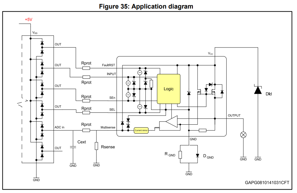
Datasheet shows \$D_{ld}\$ between \$V_{CC}\$ and GND, which I do not see in your schematic. There is no info on this diode in the data sheet.

enter image description here

From AN1596 - APPLICATION NOTE VIPower: HIGH SIDE DRIVERS FOR AUTOMOTIVE

Protection against low energy spikes and load dump

this occurs when the battery is disconnected whilst being charged by the alternator. The voltage spike can reach duration of approximately ½ second and it is of high-energy nature because of the alternator's low source impedance. Where a centralized clamp circuit is not provided or ISO7637 rated devices are not used, an external zener Dld diode is necessary to clamp the transient voltage battery (see figure 7). This is done because an internal protection against load dump would require a larger die size and - therefore - higher cost than putting on a module level protection.

Now the source is not a battery and the load is not inductive, but you are going from 7.5A to 0. No idea, what impact this would have on a power supply, but no \$D_{ld}\$ does not offer any protection and may be part of your problem.

\$\endgroup\$
7
  • \$\begingroup\$ Thank you for the answer. Could you please provide an answer for this follow up question : electronics.stackexchange.com/questions/517322/… \$\endgroup\$
    – user220456
    Commented Aug 23, 2020 at 16:20
  • \$\begingroup\$ That is something you have to sort out. It is the job and there are no shortcuts. Ideally, you will have a testbed of microcontroller software to allow you to focus on specific datasheet numbers. Vary power supply withing range and retest. What impact does ambient temperature have on numbers? Run a setup forever, switching load off and on. \$\endgroup\$ Commented Aug 23, 2020 at 16:40
  • \$\begingroup\$ Thank you. Just wanting to what are the specific tests that one needs to perform with that IC. I am not sure where to share and approach. So, I am doing random tests like I mentioned in this question. Don't know whether its right or wrong. So, I am looking for some specific advice on what are the test cases that I need to perform. \$\endgroup\$
    – user220456
    Commented Aug 23, 2020 at 17:29
  • \$\begingroup\$ It's all driven by micro, so hard to see anything critical. \$\endgroup\$ Commented Aug 23, 2020 at 19:26
  • \$\begingroup\$ Are you saying that nothing can be tested \$\endgroup\$
    – user220456
    Commented Aug 24, 2020 at 1:01

Your Answer

By clicking “Post Your Answer”, you agree to our terms of service and acknowledge you have read our privacy policy.