2
\$\begingroup\$

Hello and thanks beforehand. I have this document in altium that has some weird issue with some vias. As you can see in this photo, some vias are like greyed out on the grey part, and they are not affected by the clearance rules between the vias and the polygon pours. However, i cannot think what is the problem with those vias since the properties between those vias and the correct ones (line the one on the bottom left corner) are exactly the same. By replacing those vias with a copy of a normal one everything goes back to normal but there are a lot of them and i would rather know what causes this. DRC does not throw any errors which is what bugs me the most. It only happens in one layer for each via, so if one via is greyed out in one layer it won't be for the rest of the layers.

weird vias example

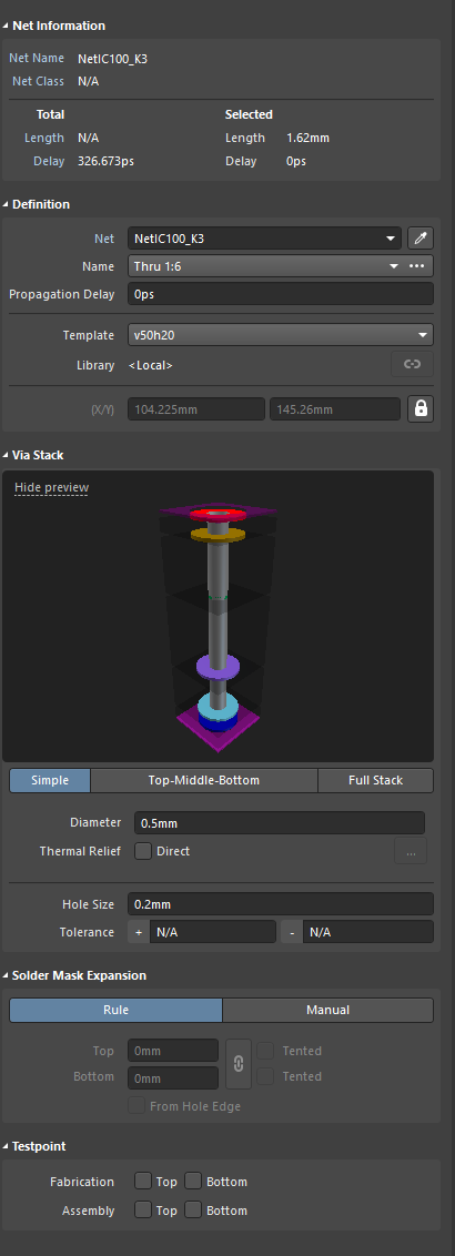
This are the properties of a normal via

Normal via

And this are the properties of a greyed out via.

Greyed out via

\$\endgroup\$
1
  • 2
    \$\begingroup\$ if the properties are exactly the same, then why is the via stack different? \$\endgroup\$
    – jsotola
    Commented Oct 6, 2020 at 16:15

1 Answer 1

1
\$\begingroup\$

It is unclear what you refer to as "greyed out", but for instance, the via on the left(GND) is not "greyed out", but it simply does not have a pad/annular ring on this layer:

enter image description here

The dark area (which is what I'm thinking you are referring to as "greyed out") is simply an area without copper.

This is consistent with the Via Stack you posted and at which jsotola's comment hints at.

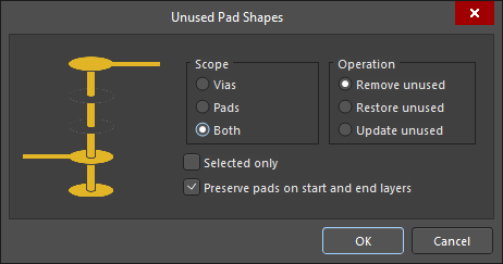
One way of obtaining such vias is editing the stack manually, changing the diameter for each layer. Another option is to use the "remove unused pad shapes":

To remove unused pad shapes, select Tools » Remove Unused Pad Shapes

enter image description here

From Altium documentantion.

Some reasons to remove unused pad shapes:

1 - Leave more copper on the desired layer (since unconnected vias do not have annular rings)

2 - Gives more space in inner layers if clearance is a concern

3 - Less copper to drill through helps lengthen drill bit life

Honestly, 90% of the reason for me to do it is the first one, but I guess it will vary depending on who you are.

Also worth noting that due to the way plating works, its not possible to remove the Via shapes on first/last (top/bottom) layers.

This seems poorly documented/discussed so take it with a grain of salt: It seems that removing unused pads increases reliability for PCBs that suffer intense thermal cycles (but apparently it also reduces reliability in other contexts).

\$\endgroup\$
1
  • 1
    \$\begingroup\$ That's it! thanks a lot. What happened is that some of those removed pads had to be updated and that's why I was having problems. This explains everything. Thanks a lot again. \$\endgroup\$ Commented Oct 7, 2020 at 10:36

Your Answer

By clicking “Post Your Answer”, you agree to our terms of service and acknowledge you have read our privacy policy.

Not the answer you're looking for? Browse other questions tagged or ask your own question.