3
\$\begingroup\$

While I have found a few resources (here here here) describing the coverage (strive for 100 %!), distribution (avoid clustering, at least 100 mil apart, away from tall components), and size (40 mil if you can) of test points designed for bed of nails in-circuit testing (ICT), I have not found guidance on the placement of them among traces.

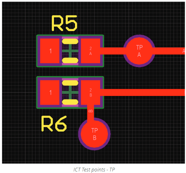
I have seen some pretty ugly placement -- e.g. test points tangential to traces or halfway across the board from their signal's main trace -- but the two options I notice the most are directly inline with the trace or close by the trace/component and bridged with a short trace:

Typical test point locations

The former (TP-A above) makes the most sense to me while the latter (TP-B) looks to be a technique used among a high density of traces and test points (I'd also be more concerned with acid traps here, but it seems like modern manufacturing techniques aren't as vulnerable). Are there guidelines or best practices that relate here?

\$\endgroup\$
1
  • 2
    \$\begingroup\$ I don't know of any official guidelines, but I've seen it done both ways like you describe. I would think the placement is more a mechanical thing... Make sure the bed-of-nails can actually make contacts w/o hitting something. Also, version "A" above can make laying parallel traces difficult on a really packed board due to the other traces having to meander around it. Ultimately, I can't imagine any reason to prefer one over the other for 'electrical' reasons unless you're probing signals operating at very high frequencies. But I look forward to hearing others thoughts! Good question! \$\endgroup\$
    – Kyle B
    Commented Jan 26, 2021 at 21:29

1 Answer 1

2
\$\begingroup\$

There are no rules for placement of testpoints because the main point is to check the value of a component or at least its presence. The EMS requires testpoints so it can check that it put correct components in place. If you don't put testpoint, EMS can't check the PCB assembly, so any defect would be your responsability as you didn't provide any means to check the assembly.

The EMS is not a PCB designer and usually don't know anything about the PCB's function. Thus it only provides mechanical guidance regarding testpoints. The location and pad design is up to the PCB designer. Most of the time testpoints are present on low speed signals, so location and size doesn't matter that much : a small stub on an enable signal is not a problem. Same for an I2C signal with a testpoint on the trace, yeah there will be an impedance change but at 400kHz it shouldn't be an issue.

Issues arised when you have critical signals or when you need precise mesurement, then location and size of the test point is something to look for and sometime accept that you won't put testpoints and maybe choose another way.

Usually you try to put your testpoints in via holes so it doesn't involve specific testpoint pad, you just need to check the via pad size and hole diameter with the EMS so it can be used as a testpoint. Then for testpoints pads, the more critical the signal, the shorter the stub.

Finally, on advanced components you should be able to test your traces through Boundary Scan and related technologies.

\$\endgroup\$
2
  • \$\begingroup\$ Can you expand the EMS acronym? I'm not familiar. \$\endgroup\$ Commented Apr 7, 2021 at 14:19
  • \$\begingroup\$ EMS = Electronics manufacturing service. It might be a bit larger than PCB assembly and test as an EMS can also do assembly and test of the final product. en.wikipedia.org/wiki/Electronics_manufacturing_services \$\endgroup\$
    – zeqL
    Commented Apr 7, 2021 at 16:35

Your Answer

By clicking “Post Your Answer”, you agree to our terms of service and acknowledge you have read our privacy policy.

Not the answer you're looking for? Browse other questions tagged or ask your own question.