3
\$\begingroup\$

I'm using a 74LVC245 buffer, which is a 3.3V chip with 5V tolerant inputs. What will happen if one of the chip's outputs is enabled and is connected to an external device with a 2K pull-up resistor to 5V? I welcome suggestions on other ways to do this, but I'm mainly interested in analysis of what happens with this specific setup.
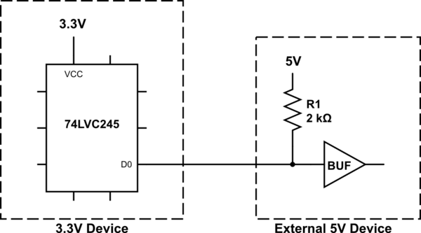
schematic

simulate this circuit – Schematic created using CircuitLab

The 74LVC245 datasheet states that the voltage range applied to any output in the high or low state must be between -0.5V and VCC + 0.5V. There's also a footnote that says the output negative-voltage rating may be exceeded if the output current rating is observed. I assume this refers to the output clamp current, which is -50 mA for Vo less than 0V.

Here's where I'm confused. Whether the D0 output is either driving high or low, there will be a voltage drop across R1. Won't that keep the voltage at D0 always within the range allowed by the datasheet? If D0 is outputting a logical low value, the voltage will be 0V and current will be -2.5 mA (5 / 2K). If D0 is outputting a logical high value, the voltage will be 3.3V and current will be -0.85 mA (1.7 / 2K).

I'm particularly unsure about what happens when D0 is a logical high value at 3.3V. Current will be flowing into D0 - where does it go, and through what structure in the chip? Is there a clamp diode to the 3.3V supply here? The fact that the datasheet gives a spec for max clamp current below 0V but not above 3.3V makes me think there is not a positive clamp diode. So does the current just flow into the 3.3V supply through the output transistor? Is it likely to cause problems to have a small backfeed current like this, or is 0.85 mA too small for most worries? If it matters, this is a hobby-level project, not a scientific application requiring stringent specs.

\$\endgroup\$
1
  • 1
    \$\begingroup\$ There is the 74lvc8T245 that will provide the translation for you. Not pin compatible though. Or a 74hct245 running on 5V as long as it is only used in one direction. \$\endgroup\$
    – Kartman
    Commented Jun 25, 2021 at 8:33

2 Answers 2

3
\$\begingroup\$

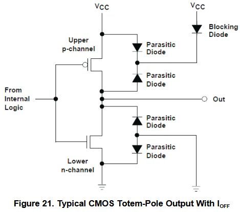
CMOS outputs are impemented with MOSFETs, which have parasitic body diodes.

However, the LVC logic family has "IOFF" circuitry to prevent a current from flowing into an output when the power is off. A current can flow into such an output only if it actively drives low or high; that current flows through the active MOSFET into GND or VCC.

LVC output with IOFF
(source: TI's How to Select Little Logic)

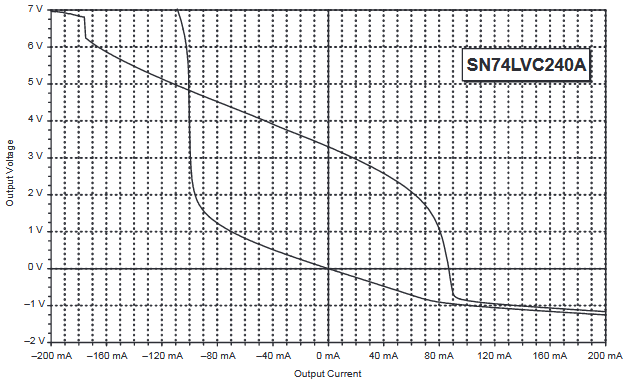
The datasheet specifies a current limit only for negative excess voltages because that limit applies to the diode between GND and the output; no such diode is active for positive voltages. If you apply a voltage above VCC to an output driving high, the current is limited only by the MOSFET's impedance:

LVC output voltage vs. output current
(source: TI's Input and Output Characteristics of Digital Integrated Circuits at 3.3-V Supply Voltage)

Current flowing into VCC is usually a bad idea, because most power supplies cannot sink current. You could use a Zener diode (or better a TL431) to clamp the voltage, or connect a 3.3 kΩ resistor between 3.3 V and GND to shunt the excess current to ground.

If this is not a bidirectional bus, consider using a buffer with open-drain outputs (e.g., 74xx07); the pull-up ensures that the 5 V device sees a valid high level. Alternatively, use a level shifter to get proper 5 V signals.

\$\endgroup\$
3
  • \$\begingroup\$ Out of curiosity, when would the max output voltage rating of VCC + 0.5V ever come into play? If the pull-up were 10 ohms instead of 2K ohms, I think the output voltage would still be 3.3V but the current would be high enough to be a major concern. I can understand why the chip would have a max current rating, but not why the VCC + 0.5V rating is there or what it pertains to physically. \$\endgroup\$
    – bmow
    Commented Jun 25, 2021 at 18:35
  • \$\begingroup\$ That "0.5 V" looks like a diode drop, but there is no diode. It might be an attempt to limit the current, but there already is a current limit. There is no good explanation. \$\endgroup\$
    – CL.
    Commented Jun 25, 2021 at 19:23
  • \$\begingroup\$ @CL. the 0.5 in the driven output case might just be a copy paste from the undriven case, where there is a diode. \$\endgroup\$
    – mbrig
    Commented Jun 25, 2021 at 19:28
3
\$\begingroup\$

Here's where I'm confused. Whether the D0 output is either driving high or low, there will be a voltage drop across R1. Won't that keep the voltage at D0 always within the range allowed by the datasheet?

Yes, but it will do it by injecting current into Vcc via the upper output FET when the output is high. This won't hurt the clamp diodes, because it doesn't have any (though it probably does have Zener diodes to clamp the maximum voltage to ~7 V).

The only problem is the injected current will flow into the 3.3 V regulator, possibly causing the voltage to rise above 3.3 V. 0.85 mA isn't much, but over 8 bits it could be up to ~7 mA which may be significant in a low power circuit. Furthermore, when switching from input to output it will have to discharge the parasitic capacitance of the bus from 5 V to 3.3 V, which could introduce a large positive spike onto the 3.3 V supply rail.

So you have to ask yourself:-

  1. Can my 3.3 V supply handle the injected current?

  2. Why do I need to pull the data lines up on a bidirectional bus anyway?

\$\endgroup\$
2
  • \$\begingroup\$ For this application the buffer is always used in one direction, not bidirectionally. Only one pin will have a pull-up on its output. Yes there are likely better parts to use for this, but I appreciate the analysis specific to the 74LVC245. Thanks! \$\endgroup\$
    – bmow
    Commented Jun 25, 2021 at 18:43
  • \$\begingroup\$ If it's only one pin you will probably get away with it. Just make sure the load on the 3.3V supply is always at least 0.85mA, and have plenty of bypass capacitance. \$\endgroup\$ Commented Jun 25, 2021 at 21:58

Your Answer

By clicking “Post Your Answer”, you agree to our terms of service and acknowledge you have read our privacy policy.

Not the answer you're looking for? Browse other questions tagged or ask your own question.