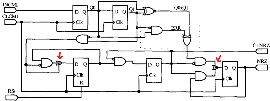
I'm studying the CMI decoder circuit from Maniatopoulos, Antonakopoulos and Makios, 1995, but I can't understand some symbols in the diagram. They look like a small logical OR. Can anyone tell me what they mean?
\$\begingroup\$
\$\endgroup\$
3
-
\$\begingroup\$ Or "expanded" ... The right "seems" to short the two output gates. \$\endgroup\$– Antonio51Commented Oct 20, 2023 at 8:11
-
2\$\begingroup\$ Hello and welcome ... the convention at EE.SE is to give references, ideally with links, for where images and so on come from ... often this helps just by giving context.. \$\endgroup\$– jonathanjoCommented Oct 20, 2023 at 8:22
-
3\$\begingroup\$ The 1995 source paper says it was implemented in ECLinPS ... could it be a wired-OR? \$\endgroup\$– jonathanjoCommented Oct 20, 2023 at 8:54
Add a comment
|
1 Answer
\$\begingroup\$
\$\endgroup\$
2
It's a notation denoting deliberately connecting two (or more) outputs together in a wired-OR configuration. This "gate" does not involve any additional components.
This is especially effective in emitter-coupled logic, where the output currents simply add without causing any "fights" among the output drivers.
-
\$\begingroup\$ The instance of the symbol on the right side of the diagram makes sense as being a wired-OR configuration, but the instance on the left is confusing to me. It appears to be implementing
X OR (NOT(X) AND Y). isn't this the same asX OR Y? \$\endgroup\$– effectCommented Oct 20, 2023 at 20:11 -
1\$\begingroup\$ @effect: Yes, but the gate to the left of that is acting as a buffer for the FF's Q output. It couldn't be tied in directly, because it is also used elsewhere. That was probably the most convenient way to "tie off" the NOT input of that buffer gate. Logic like this tends to be full of implementation details that don't make a whole lot of logical sense. \$\endgroup\$ Commented Oct 20, 2023 at 21:50

