1
\$\begingroup\$

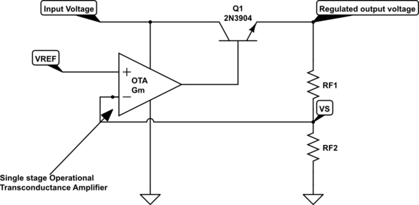
I am building a discrete voltage regulator, centered on a differential pair with an active load.

I have seen the single stage differential pair being called an Operational Transconductance Amplifier. I believe I understand how an OTA is supposed to work: $$I_{out}=G_{m}\cdot \left(V_{ref}-V_{s}\right)$$

In researching voltage regulators based on OTAs, as opposed to op amps, I've encountered only LDO with PMOS pass elements. For component availability purposes I will not be using MOSFETs, only bipolar transistors.

From my understanding, a voltage regulator is more or less an op amp/ OTA buffered in such a way to increase its maximum current output and lower its output impedance.

schematic

simulate this circuit – Schematic created using CircuitLab

$$V_{out}=\left(1+\frac{R_{f1}}{R_{f2}}\right)\cdot V_{ref},\quad \beta \geq 100$$

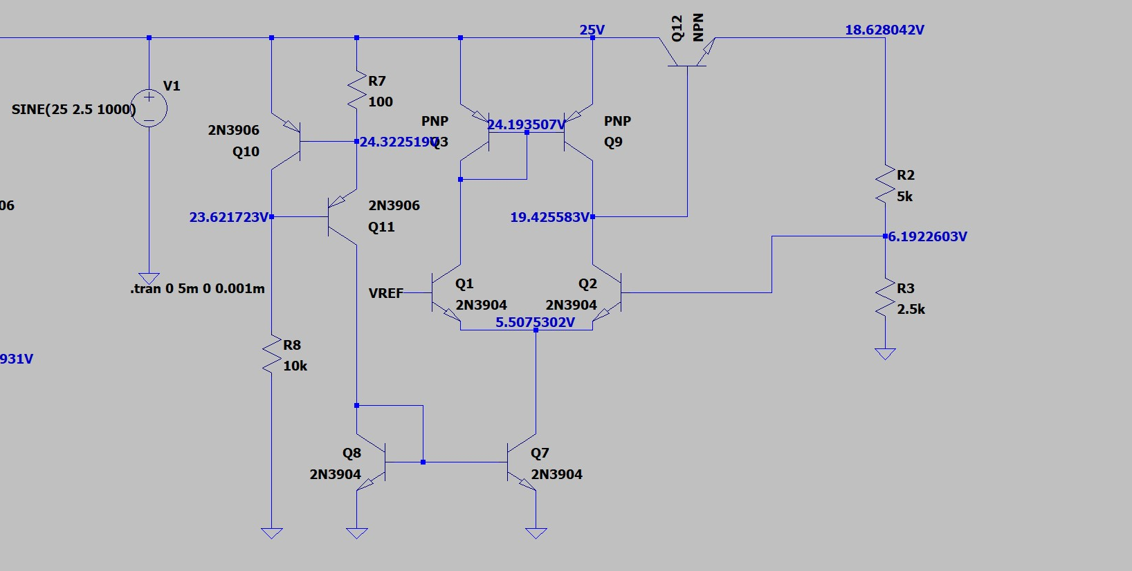
This is how I've simulated it in LTspice (Zener based voltage reference not shown):

enter image description here

Is this a sensible approach or should I try something else?

\$\endgroup\$
17
  • 1
    \$\begingroup\$ Yes but you don't need all that constant current biasing circuitry. Your operation point is fixed, so a simple resistor instead of Q7 will do. \$\endgroup\$
    – tobalt
    Commented Oct 31, 2023 at 16:22
  • \$\begingroup\$ @tobalt As I understand it, the purpose of the constant current biasing in such a circuit is to, among other things, enhance CMRR and PSRR. Theoretically I could even get rid of Q9 and Q3 and still have a functional OTA. \$\endgroup\$ Commented Oct 31, 2023 at 16:27
  • \$\begingroup\$ And perhaps to make it even closer to a theoretical transconductance amplifier, I could swap the transistors in the differential pair with Darlingtons to increase the input resistance, but that's too much complexity for me right now. \$\endgroup\$ Commented Oct 31, 2023 at 16:29
  • \$\begingroup\$ Again, CMRR is irrelevant because your op point is constant. Q3 and Q9 enhance gain, so those are quite useful. But the biasing circuit justs sets the op point, which a single resistor (that will give you the same tail current) will just as well. Just compare the performance in spice. \$\endgroup\$
    – tobalt
    Commented Oct 31, 2023 at 16:36
  • 1
    \$\begingroup\$ The open loop gain will be load resistance dependent. And it will be in the range of Aol = gm * (beta + 1)*RL \$\endgroup\$
    – G36
    Commented Oct 31, 2023 at 17:49

2 Answers 2

1
\$\begingroup\$

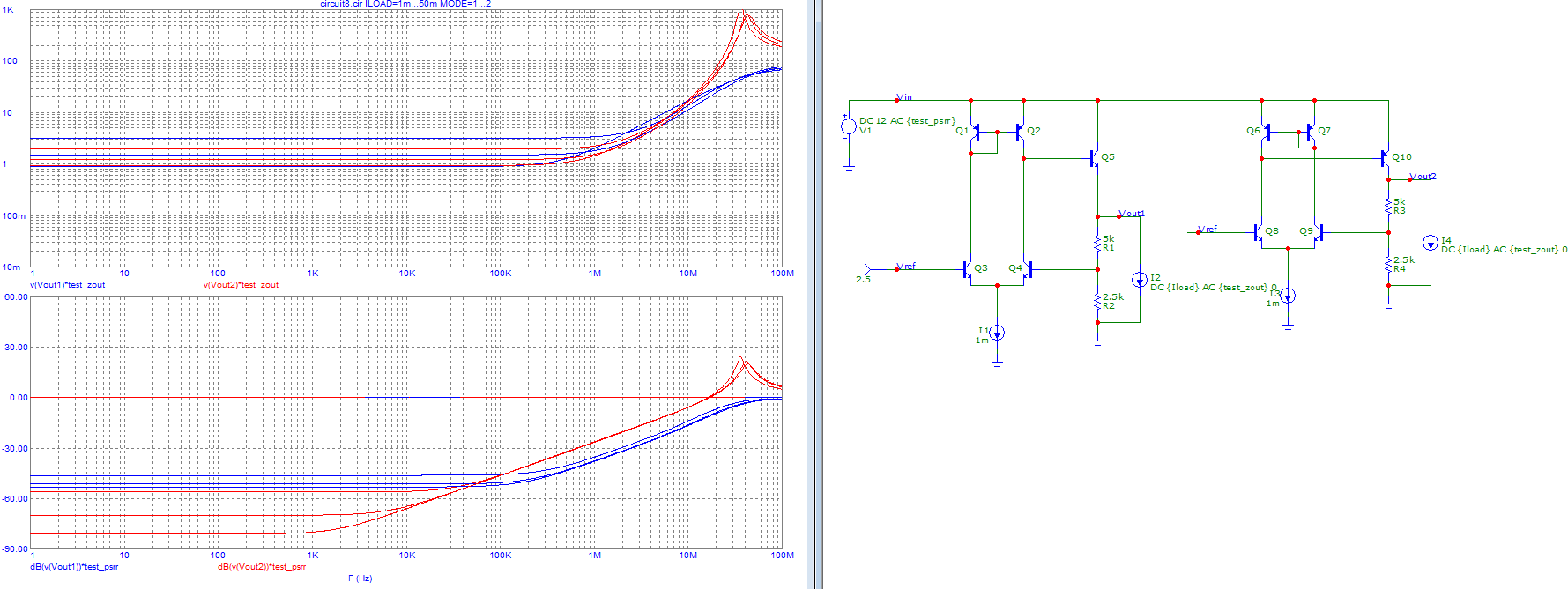
Let's check output impedance (top plot) and PSRR (bottom plot) of both PNP and NPN pass transistor versions of this regulator.
enter image description here

Left (NPN) in blue ; right (PNP) in red ; 3 output current steps (1mA,20mA,50mA).

In both circuits the pass transistor (Q5 or Q10) acts purely as current gain. It is not a voltage follower, even in the NPN case, because its input voltage is not controlled, coming from the meeting point of two collectors.

Therefore the circuit dumps into the load a current that is the product of hFe of the pass transistor, multiplied by gm of the input stage, multiplied by error voltage at the input of the LTP, which is the error voltage at the output times the voltage divider ratio. So the DC open loop transconductance is...

  • gm = about 20mS at collector current of 500µA per transistor
  • hFe ~180 for 2N3904 spice model
  • 1/3 for the feedback divider

Which gives a product of 1.2S as transconductance for the whole circuit. Output impedance is the inverse: 0.83 ohms, which is quite close to the "around one ohm output impedance" on the plot.

This is quite high, for good regulation you need lower output impedance than this so this isn't an acceptable LDO: it doesn't have enough open loop gain.

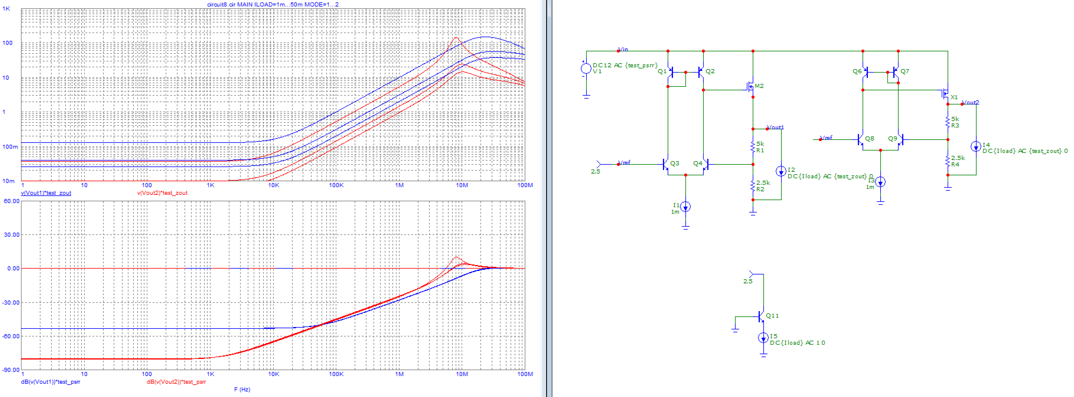
Let's substitute BJT pass transistors with FETs.
enter image description here

This simple change reduces output impedance by orders of magnitude, at least at low frequencies. This is due to the FET having no DC gate current so at low frequency its current gain is much higher than the hFe of a BJT. The formula to calculate output impedance is the same as above, but with the FET's much higher current gain, transconductance is much higher and thus output impedance is much lower.

Not everything is well and good though, because between 10k-1Meg the output impedance is inductive and that's where we want to cross over with the output cap, so it will probably be underdamped and be a special snowflake LDO that requires an output cap with just the right ESR for damping.

how the output impedance of the circuit relates to the loop transconductance

The circuit is an OTA (output transistor included): its output current is proportional to the error voltage at the output, and the proportion factor is transconductance. Since transconductance is dIout/dVout and output impedance is dVout/dIout, one is the inverse of the other.

In the document you linked, the SiC regulator uses collector resistors in the input stage instead of a current mirror. So the input stage doesn't output a current, it outputs a voltage, and the pass transistor doesn't act as pure current gain, instead it's a follower. So loop gain calculations are different.

inductive output impedance.

In the question (and in the linked document) loop gain and transconductance are only studied at DC, ie "0 Hertz". Plotting output impedance versus frequency shows that it rises at a slope of 20dB/decade, just like the impedance of an inductor would.

This is due to the main pole, which is due to input capacitance and Miller effect in the FET pass transistor. This FET is driven by current from the current mirror, and this current is integrated into a voltage by its input capacitance. This creates a pole and loop gain decreases by 20dB/decade.

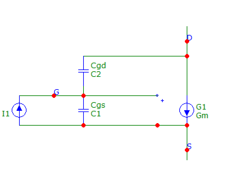
To understand frequency dependent effects I feel the following analogy works well:
enter image description here

If you drive the device with a current (from I1, having DC and AC components) then this current is integrated into an AC voltage Vgs by the input capacitance. Vgs then drives the output current through the device's transconductance gm. Current gain can be defined just like for a BJT: drain current divided by gate current, and in this case it decreases by 20dB/decade with 90° phase lag.
\$\endgroup\$
10
  • \$\begingroup\$ Judging the regulator's output impedance at light load is a bit disingenuous: diff pair current is equal to load current! Increasing it will increase the output's gm, giving a more favorable measure. Conversely: at all of 1mA, I'd be more than happy to call 1Ω a "good" regulator! \$\endgroup\$ Commented Nov 1, 2023 at 1:06
  • \$\begingroup\$ if they insist on not using a FET and if you don't want to recommend a PNP for the compensation issues, one more interesting variation of the output transistor could be an n-type Darlington or Sziklai arrangement. \$\endgroup\$
    – tobalt
    Commented Nov 1, 2023 at 4:19
  • \$\begingroup\$ First of all, thank you for taking the time to simulate my circuit. I understand how you obtained the dc open loop transconductance. I don't understand the part about inductive output impedance. My calculations show that: $$V_{o}=\frac{g_{m}(\beta + 1)(R_{1}+R_{2})}{1+g_{m}(\beta + 1) R_{2}}\cdot V_{ref}$$. The product $$g_{m}(\beta + 1)$$ seems to be critical. For gm larger than unity the expression should simplify to the familiar $$\left(1+\frac{R1}{R2}\right)\cdot V_{ref}$$ \$\endgroup\$ Commented Nov 1, 2023 at 7:29
  • \$\begingroup\$ Would this mean I need to increase the tail current of the pair substantially to obtain something closer to the ideal expression. Conversely, couldn't I analyze the regulator from the POV of the loop gain? Like it's done in this document: diva-portal.org/smash/get/diva2:1073421/FULLTEXT01.pdf#page=49 \$\endgroup\$ Commented Nov 1, 2023 at 7:34
  • \$\begingroup\$ Also I am not sure I understand how the output impedance of the circuit relates to the loop transconductance. \$\endgroup\$ Commented Nov 1, 2023 at 8:41
1
\$\begingroup\$

One of the most important specifications of a voltage regulator is load regulation. When the load current varies, we ideally want the output to be constant but, in reality, there will be a change and by design, we must try to minimize this.

In your present configuration, if load current IL varies, the base current (IL/(1+beta)) varies and hence it will create an offset voltage at the input of the diffamp (IL/((1+beta)*GM)). The output voltage will have an error of (IL/((1+beta)GM)(1+Rf1/Rf2)). We do not have any good option here to reduce this error other than increase GM but that will increase diff amp current which is not usually acceptable. If we had a MOSFET in the place of the BJT pass transistor, this error component would not have been there and the load regulation would've been much better.

Edit: For such high diffamp bias currents that you have used, you may not see the load regulation issue. If you reduce the bias currents to uA range, you'll see the issue. In such a case, you can use a 2-stage amp to drive the pass transistor if you can't use a MOSFET transistor pass element.

\$\endgroup\$
4
  • \$\begingroup\$ Not using a MOSFET is one of their design parameters though... \$\endgroup\$
    – tobalt
    Commented Oct 31, 2023 at 17:41
  • \$\begingroup\$ The spice simulation of the regulator seems to look pretty good for reasonable loads. The output voltage stays pretty much the same down to 200-300 ohms, which is below my design parameters of 0.8 to 1K ohms \$\endgroup\$ Commented Oct 31, 2023 at 18:17
  • \$\begingroup\$ @Virgil_Tibbs, at 200ohm load, IL=31mA. Your diffamp's tail current is 6.8mA. So, you have 3.4mA in each arm of the diffpair. This is very high compared to IL/beta (assuming beta=200, IL/beta = 155uA) and that is why you don't see the load regulation issue. In commercial designs, we cannot afford such high bias currents in the amp. We design such that the total regulator current at no load is say 10uA for this kind of regulator. For such low bias currents, the effect that I mentioned will definitely popup. \$\endgroup\$
    – sai
    Commented Nov 1, 2023 at 2:45
  • \$\begingroup\$ Thank you for taking the time to entertain my question. I'll keep in mind your advice for future developments on my puny voltage regulator. \$\endgroup\$ Commented Nov 1, 2023 at 15:38

Your Answer

By clicking “Post Your Answer”, you agree to our terms of service and acknowledge you have read our privacy policy.

Not the answer you're looking for? Browse other questions tagged or ask your own question.