0
\$\begingroup\$

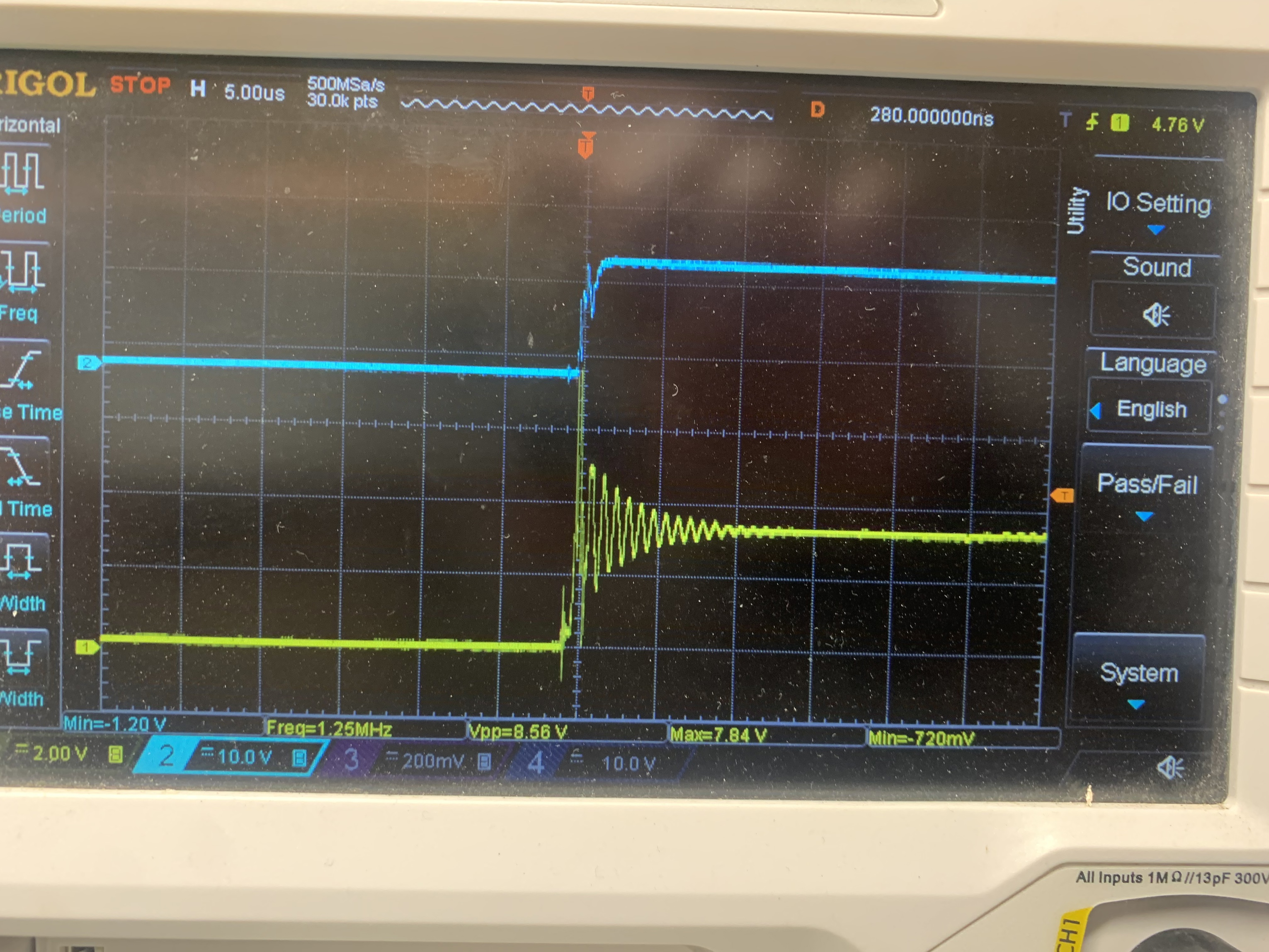
I have a 3v3 signal that has a nice sharp edge when probed in isolation. However, when I connect this to the input of a gate driver IC (TC42X series) driving a MOSFET switching an 8A load, I see strong ringing when probing the input (yellow). The logic input is supposed to draw less than 1uA. The blue trace is the gate voltage. What is happening here?

enter image description here

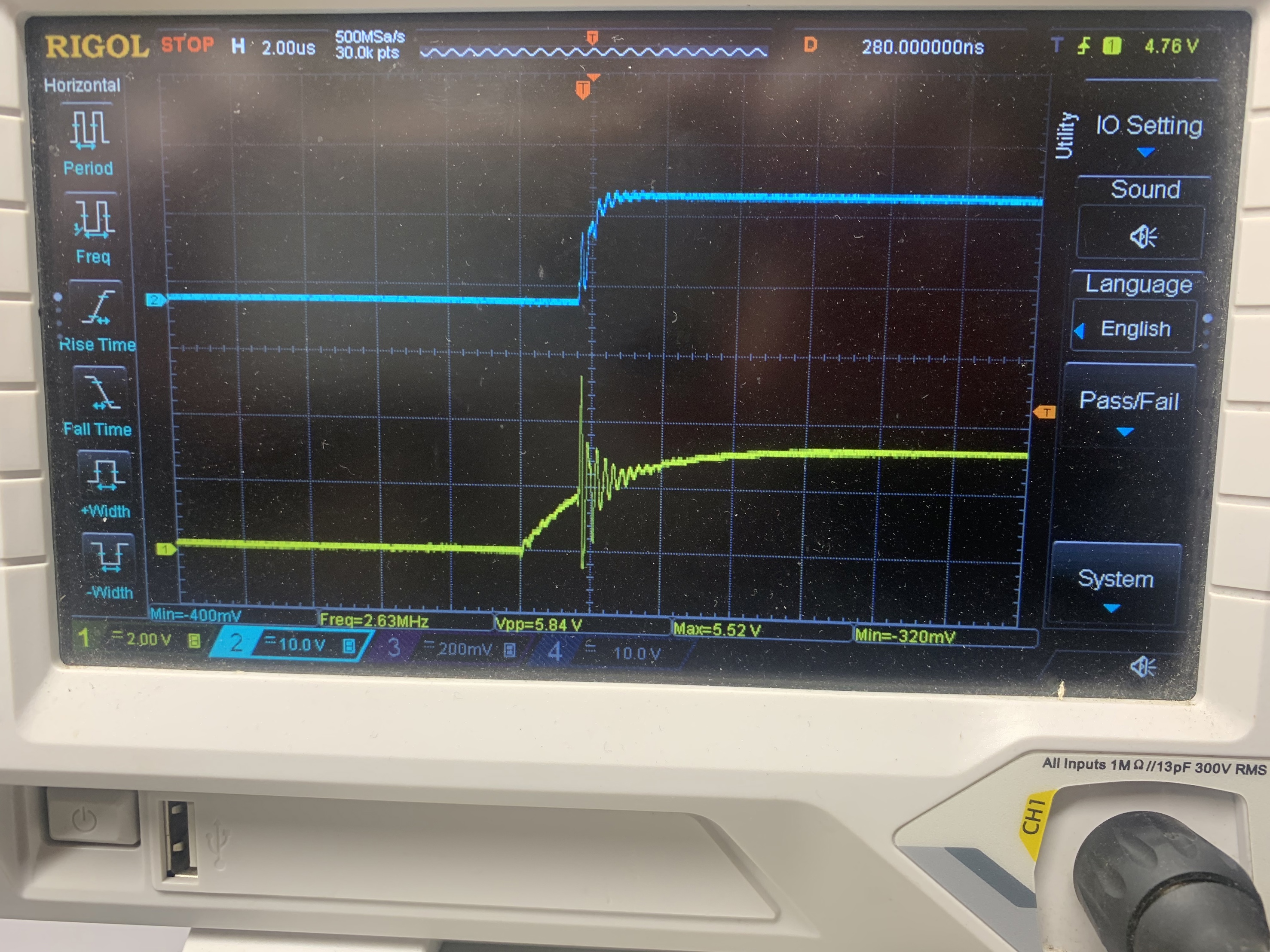
Out of curiosity I added an RC filter to the input and observe similar ringing on the input pin when the Schmidt trigger hits threshold in the gate driver. What could be the origin of this strange transient on the data line?

enter image description here

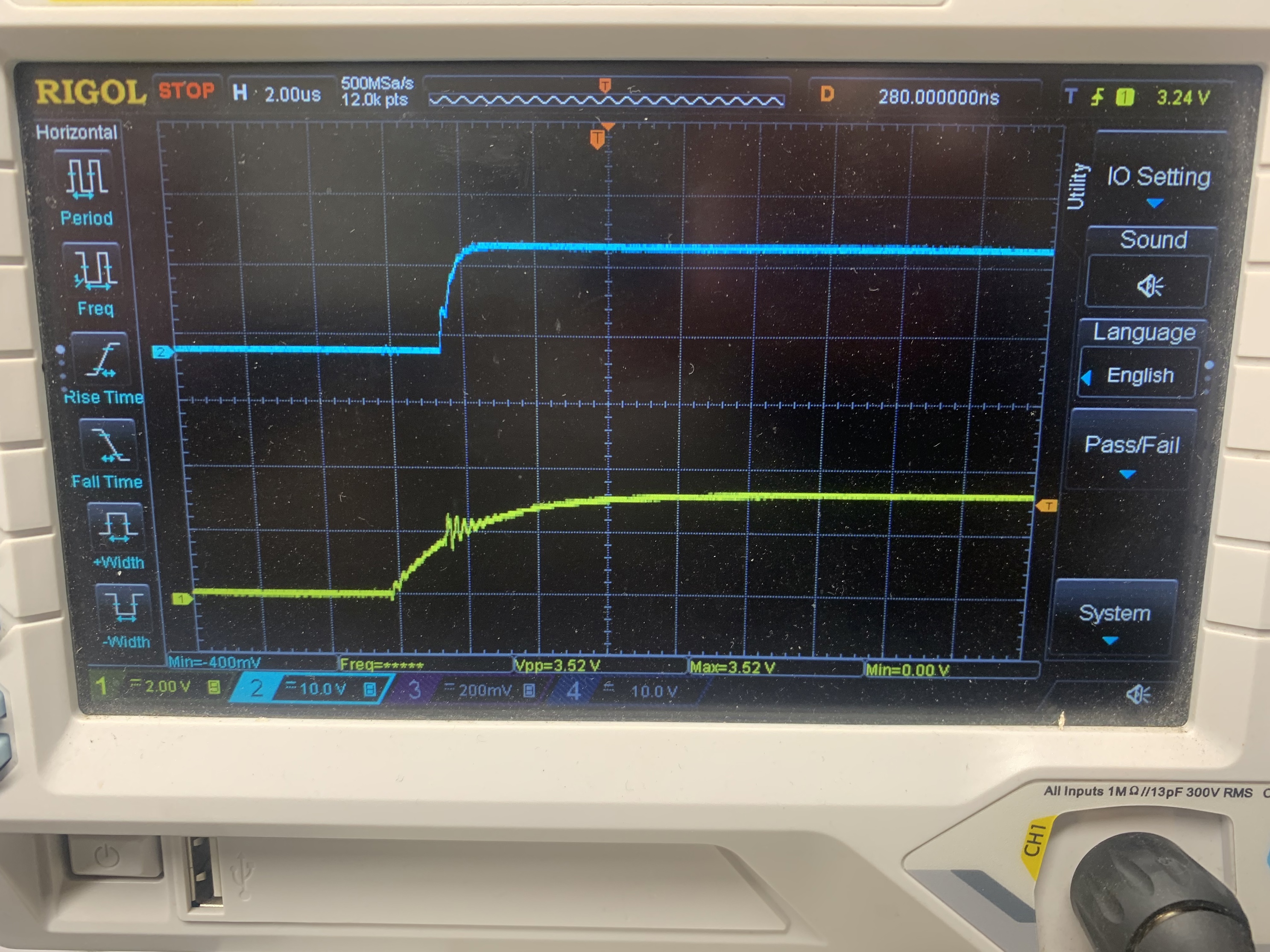
With the load disconnected it’s still there but small

enter image description here

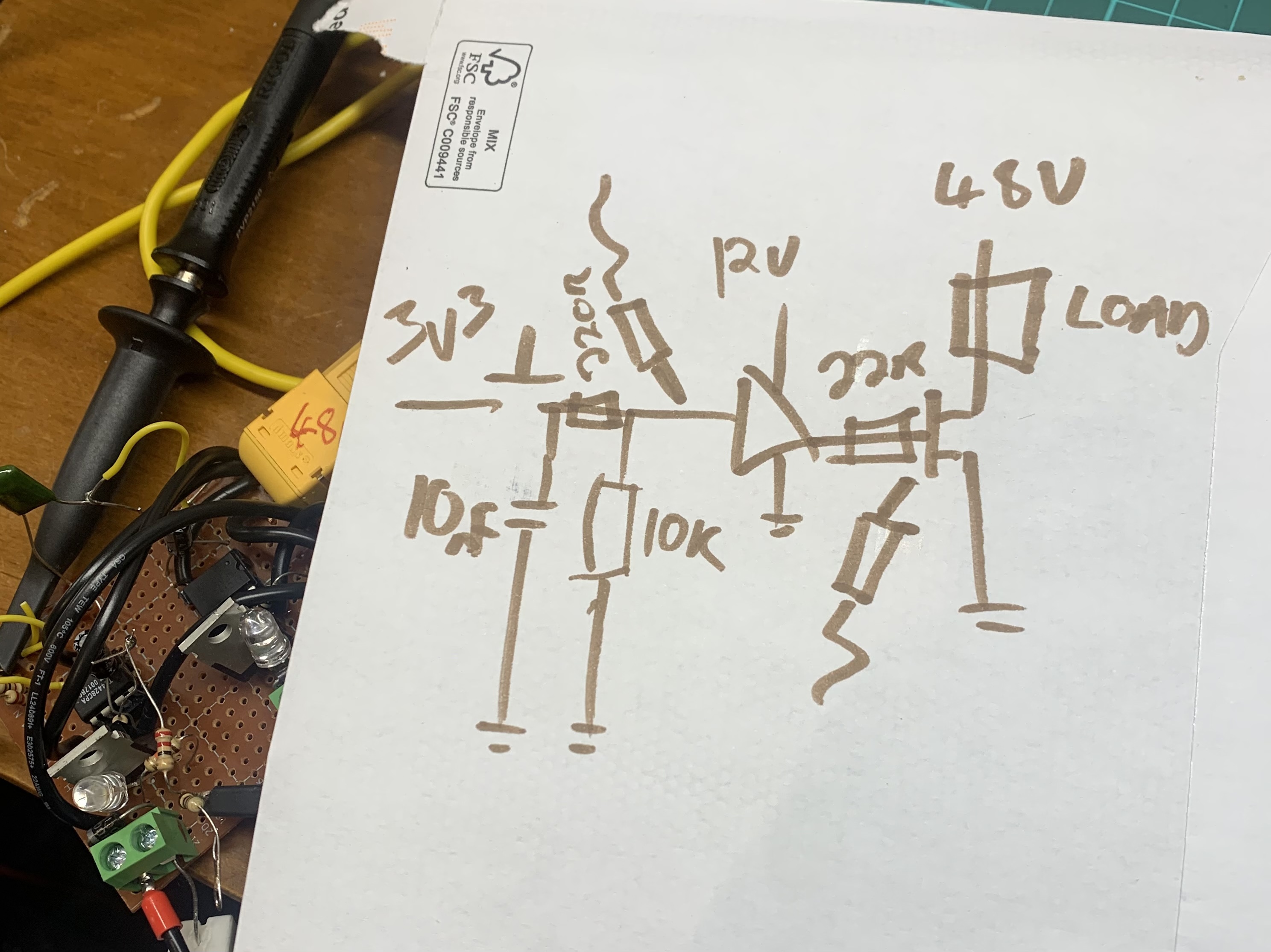
Circuit diagram below

enter image description here

\$\endgroup\$
10
  • 2
    \$\begingroup\$ Post your circuit. And a picture of your setup would be useful. Including probe location. \$\endgroup\$
    – MOSFET
    Commented Sep 13 at 1:17
  • 1
    \$\begingroup\$ Does it still show when probing circuit ground? \$\endgroup\$ Commented Sep 13 at 1:53
  • 1
    \$\begingroup\$ The probe still needs to be grounded. Earth referenced or not. You basically have an antennae. \$\endgroup\$
    – MOSFET
    Commented Sep 13 at 2:32
  • 1
    \$\begingroup\$ Oh yeah? 0.2 ohms from DUT to scope faceplate ground. At what frequency? (wink) \$\endgroup\$
    – MOSFET
    Commented Sep 13 at 2:34
  • 1
    \$\begingroup\$ Before you go down any rabbit holes, check your supply rails for ringing, first suspect is always inadequate decoupling. How are you getting your 12V and 3.3V supplies? Do they share any common voltage source? \$\endgroup\$ Commented Sep 13 at 4:11

1 Answer 1

0
\$\begingroup\$

As the FET turns on, two often-unexpected thing happen.

  1. as the drain voltage falls, the capacitance between D and G slows down the rise of VGS (Miller effect) -- this because the gate drive has to supply charge to the G-D capacitance. Thus the FET spends a long time in the high gain linear state. This can trigger ringing and oscillations in the circuit (depending on your layout; 8A and some fly-wire components on a perf. board is likely to have issues such as this).
  2. 8A switching suddenly through the FET and into the source will cause the source V to rise due to perhaps 10's of nH inductance in the GND line. This will then to turn off the FET and while usually the loop gain is below 1, the system will still ring.

To get cleaner waveforms, you should:

  1. move the 22 Ω as close as possible (mm) to the gate.
  2. try to get as close to an ideal and single GND as possible. Wire the GND of your driver to the S of the FET. If your gate driver IC doesn't have input hysteresis, then you'll also have to ensure your input control signal also refers to the same GND.
\$\endgroup\$

Your Answer

By clicking “Post Your Answer”, you agree to our terms of service and acknowledge you have read our privacy policy.

Not the answer you're looking for? Browse other questions tagged or ask your own question.