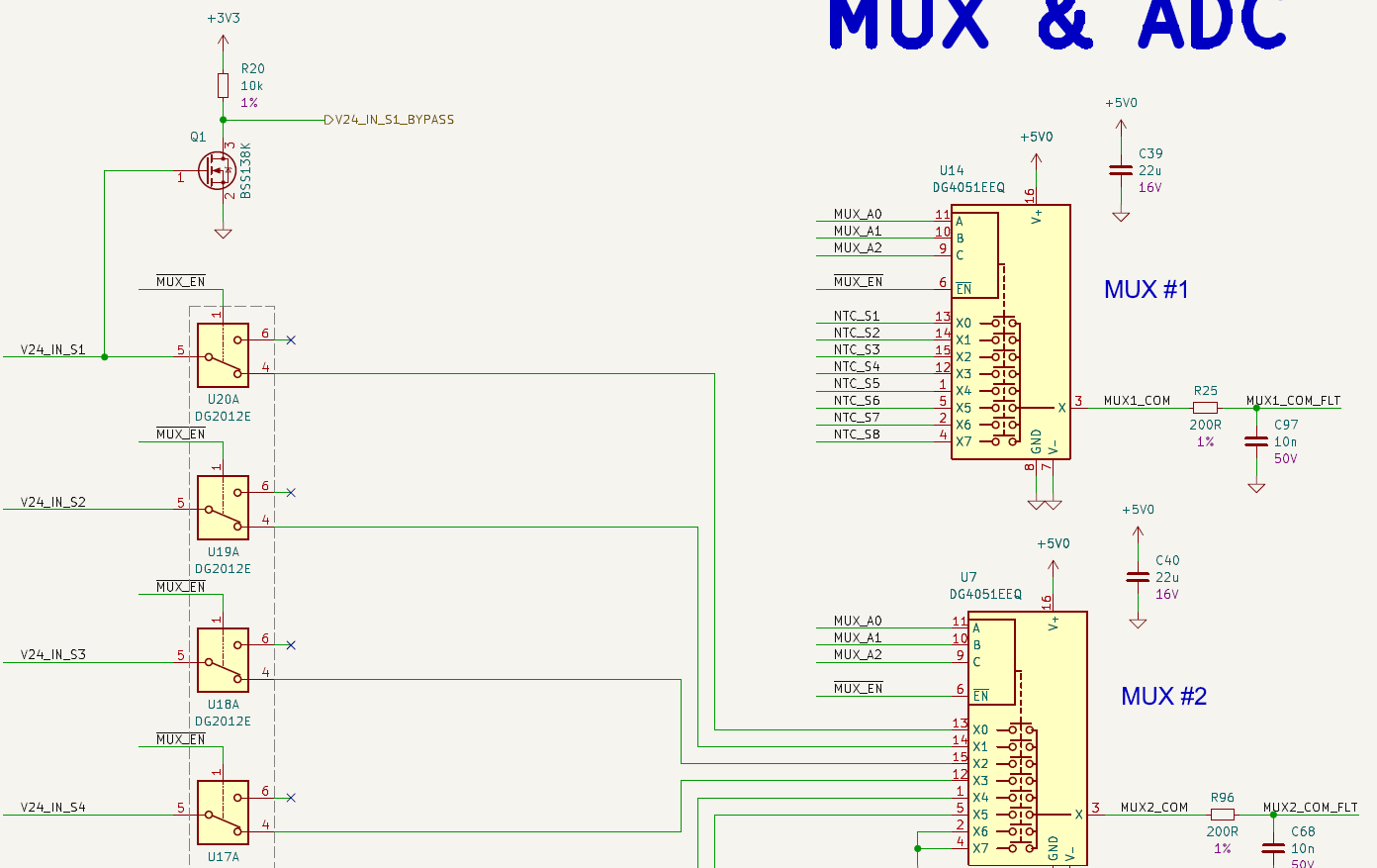
I'm using the following circuit with Q1 and R20 in order to detect 0-24V pulses that might exist on the V24_IN_S1 input:

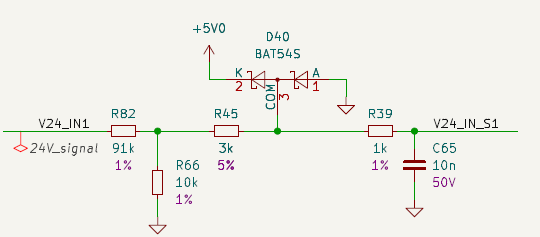
Before V24_IN_S1 there is the following circuit that transforms the 24V-level signals to lower ones:

The idea is that the pulses are converted to 0-3.3V pulses that can be detected by the MCU (an ESP32-S3) that receives V24_IN_S1_BYPASS on one of its GPIOs.
At the same time, the (analogue) signal V24_IN_S1 is driven to multiplexer and then an ADC (not shown in the diagram). MUX_EN_N (active LOW) enables or disables the MUX outputs.
What I have observed is the following:
When MUX_EN_N is HIGH (MUX output disabled and pin 5 of U20 is connected to pin 6), then the V24_IN_S1_BYPASS signal is switching, following V24_IN_S1, but its LOW level is very high, therefore the MCU always sees a digital HIGH.
When MUX_EN_N is LOW (MUX output enabled and pin 5 of U20 is connected to pin 4), then the V24_IN_S1_BYPASS signal is switching as it should, and its LOW level is close to 0, enough so that the MCU can recognize the digital LOW levels.
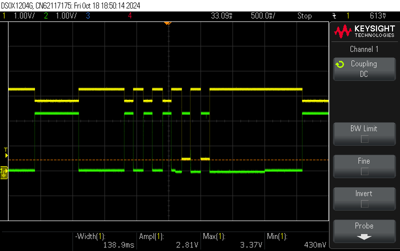
Here is an oscilloscope capture that summarizes the situation (with green color it's V24_IN_S1 and with yellow color it's V24_IN_S2_BYPASS):

You can see that in the beginning (when MUX_EN_N is HIGH), V24_IN_S1_BYPASS doesn't go all the way down to 0V. This changes a little bit after 2.5 sec, when MUX_EN_N switches LOW for a period and V24_IN_S1_BYPASS switches close to 0V.
My problem is that it is very puzzling why there is this behavior. I cannot really understand how MUX_EN_N is affecting V24_IN_S1_BYPASS.
My first thought was that perhaps Q1 doesn't open completely when MUX_EN_N is HIGH (for some reason) and that causes a high Ron, with the result we observe. However, from the waveforms, I cannot see how this is possible because the V24_IN_S1 signal puts in all cases around 2.4V across G-S of Q1. In any case, when MUX_EN_N is HIGH, U20 connects V24_IN_S1 to pin 6, so to a floating node. Compared to being connected to the MUX input, I suppose this is a less complicated scenario (less capacitance for example), therefore I would expect a problem when MUX_EN_N is LOW, if anything.
The scenario that the GPIO of the MCU where V24_IN_S1_BYPASS is connected changes to something else than INPUT (e.g., OUTPUT or INPUT with internal pull-down) is not something very likely. In any case, I've studied the code running on the MCU and I didn't see anything like this.
Any good ideas why this can be happening? Can you see any logic behind it?
UPDATE 1: I've disconnected the V24_IN_S1_BYPASS signal from the MCU (by physically cutting the trace on the board) and I still observe the same behavior. I have at least ruled out that there is some issue with the GPIO and the MCU.
