How do you represent a forbidden state of an S-R Latch (Active High) in a timing diagram?
Where S is 1 and R 1 is and C is 1. 
The forbidden state is not a specific logic level. The value of Q during the forbidden state depends on how the latch is implemented (whether with NAND gates or NOR gates, for example). There are two reasons why a particular input state may be considered forbidden. First, it may cause both Q and !Q to have the same value, which can cause undesirable effects in the logic driven by the latch outputs. Second, if the inputs transition directly from the forbidden state to the hold state, then the values of Q and !Q will be unknown. Q and !Q will eventually settle into a state where they are valid logic levels and complements of each other, but you can't predict whether Q will finally be a 1 or a 0.
So, you represent Q on the timing diagram with whatever value it has in the forbidden state. There is no standard way of representing an unknown value but it is common to put Xs in the timing diagram or draw a shaded region between the 0 and 1 levels.
A forbidden state in this case means that the output is non deterministic, i.e. unknown. An unknown state is typically drawn as two parallel lines (meaning it could be at either level).
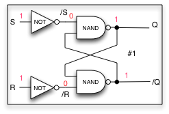
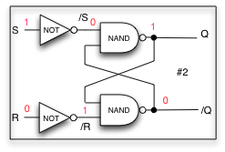
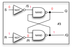
Here are the various states, I've used a NAND based latch and inverted the inputs or ease of understanding.


The red numbers are the state values. I'll leave it up to you to trace through the diagrams. Now, you have to be careful and that's why a general statement of "forbidden zone" can be misleading (some of the times).
Diagram #1: S = R = 1, gives you BOTH Q and /Q as being asserted, whereas by definition they should be complimentary to each other.
However, if you take the meaning of SET to be to assert the Q state, and you take the RESET to mean to assert the /Q state, the SET and RESET are actually doing their jobs. This might actually be OK if your down stream logic only uses one of those outputs. But it's a little more subtle than that. If you take the /Q being asserted to mean the latch is RESET then you'll be fine. However if you take the Q=0 to mean that the latch is RESET then it would be wrong. So there are two situations where it might be OK to use the signal interpret the state of the latch correctly.
It's just generally easier to to say "Thou shall not do this" - it is forbidden.
Clearly once both S & R are asserted the state is steady (non-oscillatory), but it is when S & R are transitioning to the hold state close in time to each other is when it becomes uncertain which state will win. This will depend upon the relative sizing differences in the gates themselves, and various other process variabilities. You can get race conditions between S & R and race conditions within the latch itself. But in the end this transitioning close to each other is a big statistical mess. Read up on meta-stability in latches to further your knowledge.
However, if you transition from the "forbidden state" by de-asserting either S or R with sufficient time between them (allowing for internal signal propagation) then the output will clearly be deterministic. i.e. Q = 1 for S=1 after R transitions to 0.
Here is a typical timing diagram showing the uncertain "close timing" scenario:

Do the same analysis of the state diagram for the NOR based latch. The concepts will map to different states.
In a typical single-output SR latch, the state of the output when S and R are both active will either be defined as high, or defined as low; in an SR latch with a complementary pair of outputs, the state of each output in the "R and S both active" condition may be independently defined. What is forbidden is generally not having R active while S is active, nor vice versa, but rather having them simultaneously change from the active to inactive state.