I'm attempting to design an H-Bridge which can supply 24V at 60A. As 60A is a lot of current I decided to parallel upto 4 FETs per leg to split the current.
I am using a MIC4102 2A driver to drive the FETs and I understand the important of keeping drive loop of the FETs small. Here's a circuit showing just 2 legs. The layout is also shown for the high-side.


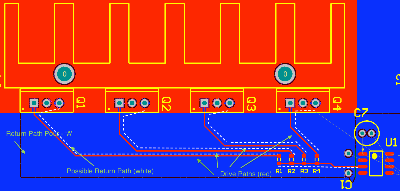
The layout shows the path from pin DH (pin 3) to the FETs' gates to their sources and back to pin HS (pin 4).
Since the high di/dt return current will try to stay close to it's drive path I decided to just pour a polygon beneath the drive traces (and resistors) and let the current flow back to the IC. I also annotated the layout picture above to show where I think the return path will flow (white dotted line in the picture). If it follows this pattern I think the drive loop will be quite small. There is a small error in the annotation - the white dotted line should go to pin 4 of the IC and not pin 3.
Can I count on this return path pour to reduce ringing that my FETs experience? Most datasheets which show a layout only show a single high-side FET and no gate resistor. The inclusion of the gate resistor and multiple FETs made it necessary for me to have polygon.
The H-Bridge (Only Half Bridge shown in schematic. The other half is exactly the same) is intended to drive a transformer at 20kHz and boost 24V upto 350V.
