0
\$\begingroup\$

I'm designing a State Variable Filter design using switched capacitors to control cut-off and resonance. Simulating this using idealized switches yields excellent results. See attached schematic Filter design with idealized switches
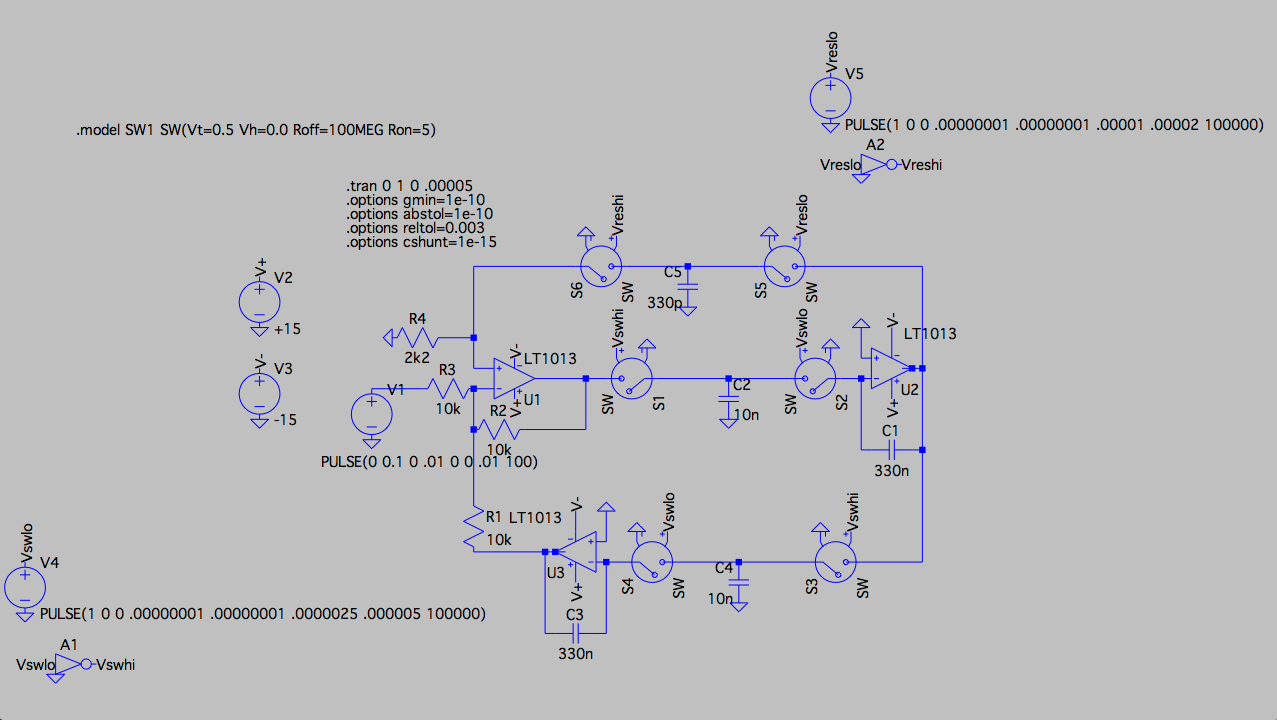
After that I proceeded to replace one of the integrators with a MOSFET version (the center-right part of the circuit). This doesn't work. I'm using a parasitic-insensitive switched cap implementation as you can see. See attached schematic Filter design with 1 integrator using MOSFETS
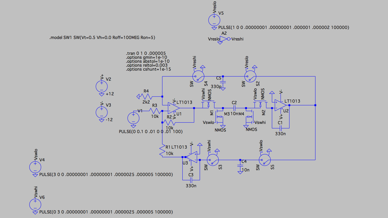
I tried a couple of implementations for the switches. First of all the parasitic sensitive version, and after that several parasitic-insensitive versions like this one. I've also tried several different NMOS models.

Can anybody tell me what I'm doing wrong here?

\$\endgroup\$
6
  • \$\begingroup\$ Why did you switch it from parasitic sensitive topology to parasitic insensitive topology? Also, you have V+ and V- giving a 24 voltage difference, while your mosfets are driven by only 3 volts. I assume the signal output swings through that range, that would prevent your signal from passing through the mosfet like a switch. \$\endgroup\$
    – horta
    Commented Jun 24, 2014 at 13:54
  • \$\begingroup\$ @horta I switched to parasitic insensitive because the sensitive version changes the integrator response. The filter still works but cutoff is lowered a lot. Indeed the clock signal needs a wider range.. quite logical! \$\endgroup\$ Commented Jun 24, 2014 at 14:46
  • \$\begingroup\$ If the cutoff got lowered, then you probably have your MOSFET gate capacitances to thank for that. Check the model of the MOSFETs you're using and ensure that the gate-drain and gate-source capacitance isn't negatively affecting your filter. \$\endgroup\$
    – horta
    Commented Jun 24, 2014 at 14:58
  • \$\begingroup\$ Add clock waveforms to your post, connect your NMOS Bulk connections properly (to ground), make sure you have NOC (Non-overlapped clocks) - especially the complements, increase voltage swing on gates \$\endgroup\$ Commented Sep 23, 2014 at 10:47
  • \$\begingroup\$ What is the modification? Why don`t you answer our questions? \$\endgroup\$
    – LvW
    Commented Dec 22, 2014 at 17:28

1 Answer 1

2
\$\begingroup\$

"Can anybody tell me what I'm doing wrong here?"

Yes - I am afraid you didn´t realize that in the second circuit (MOSFET realization) the capacitor C2 now is operated with phase inversion. That means: The most right opamp now is operating as a non-inverting integrator (besides all other effects as mentioned already).

As a result - you have positive feedback, in contrast to the first circuit (with idealized switches and another S/C realization). You can cure the situation by modifying the clock sequence for two switches.

\$\endgroup\$
1
  • 1
    \$\begingroup\$ Pieter - did you understand my above recommendation? You have produced a phase inversion around C2. \$\endgroup\$
    – LvW
    Commented Sep 23, 2014 at 12:52

Your Answer

By clicking “Post Your Answer”, you agree to our terms of service and acknowledge you have read our privacy policy.

Not the answer you're looking for? Browse other questions tagged or ask your own question.