1
\$\begingroup\$

This is a follow-up to a question I asked 3 years ago: My Coilgun Stage Driver Keeps Burning Out Mosfets. Any idea why?

I tried to take the advice in each of the answers and apply it to my circuit. But the MOSFETs still shoot through above approximately 260 V.

Here's my new test jig:

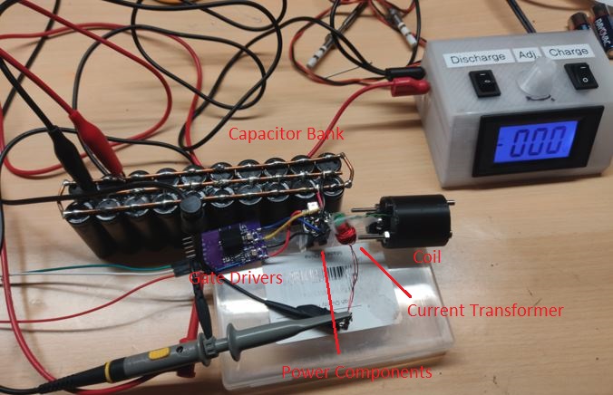
Coilgun Test Jig

Closeup of the power component pack with labels: Coilgun Power Component Pack *note, this all sits directly on top of the mosfet packages.
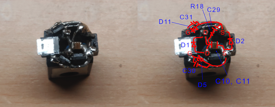
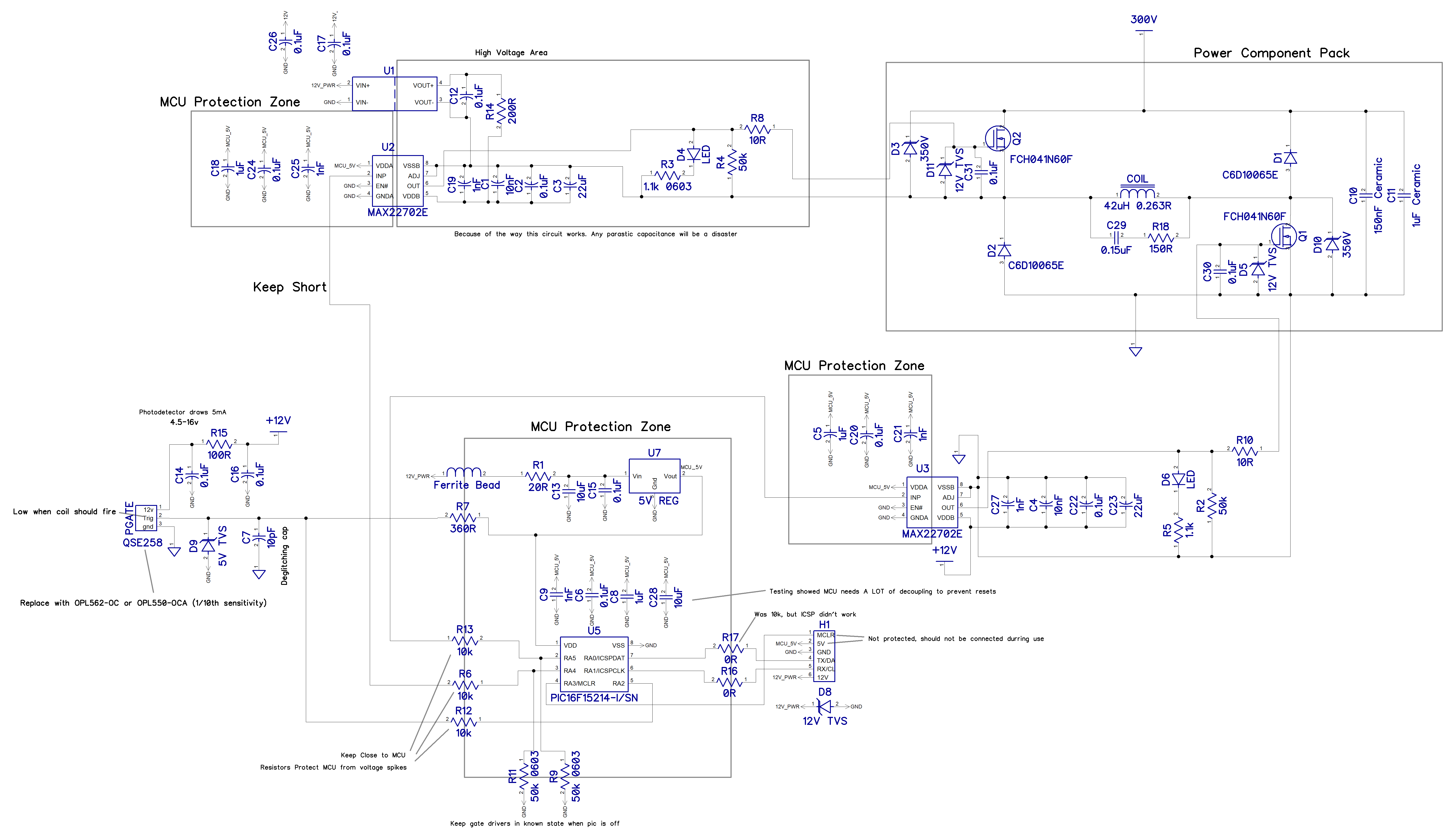
Schematic:

Coil Gun Stage Driver Schematic

Firing sequence on MCU:

HIGHFET_SetHigh();
__delay_us(10); //give high side time to turn fully on
LOWFET_SetHigh(); //turn on low side: fire
__delay_us(150); //fire time
HIGHFET_SetLow(); //turn off high side, go into freewheeling
__delay_us(100); //freewheel time
LOWFET_SetLow(); //turn off low side, go into regeneration

Improvements:

  • Shortened the wires to the cap bank as much as possible to reduce the inductance.

  • Clumped all the power components together and used very short point to point wiring to minimize parasitic inductance.

  • Added 10 ohm gate drive resistors to slow the switching.

  • Added 0.1 uF caps to the mosfet gates to dilute parasitic effects (also slows switching)

  • Added a snubber to the coil.

  • Added TVS diodes everywhere.

  • Added tons of protection around the MCU to avoid spurious resets.

  • Switched to isolated gate drivers, instead of non-isolated + optocoupler on the high side (simpler, less to troubleshoot).

Oscilloscope Traces:

Low side gate while firing at 100 V: Low side gate while firing at 100V
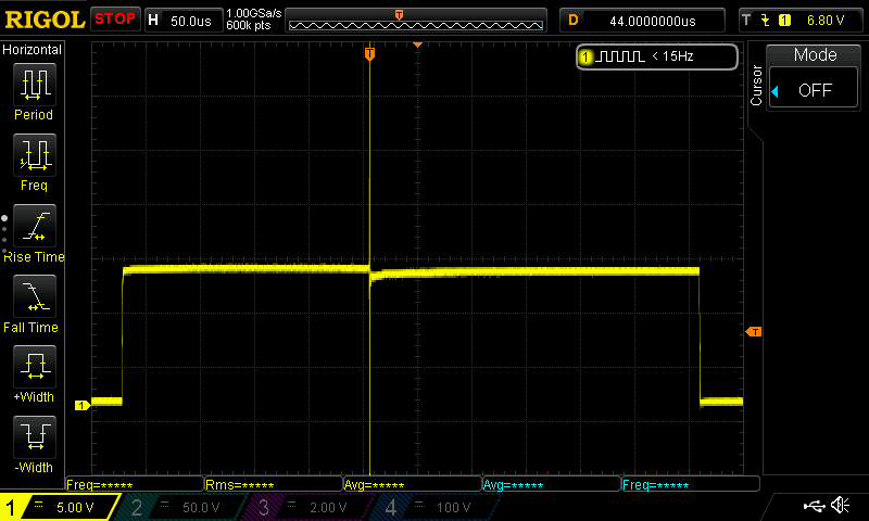
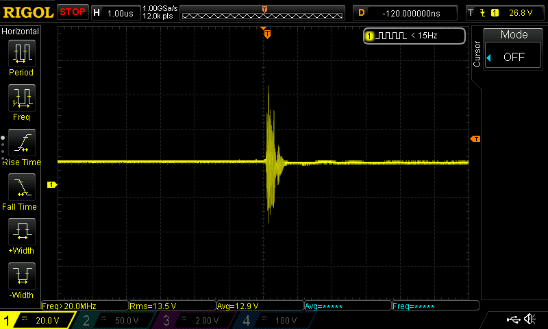
Zoomed in (new shot): Low side gate transient

Current transformer, firing at 180 V: Current Transformer firing at 180V
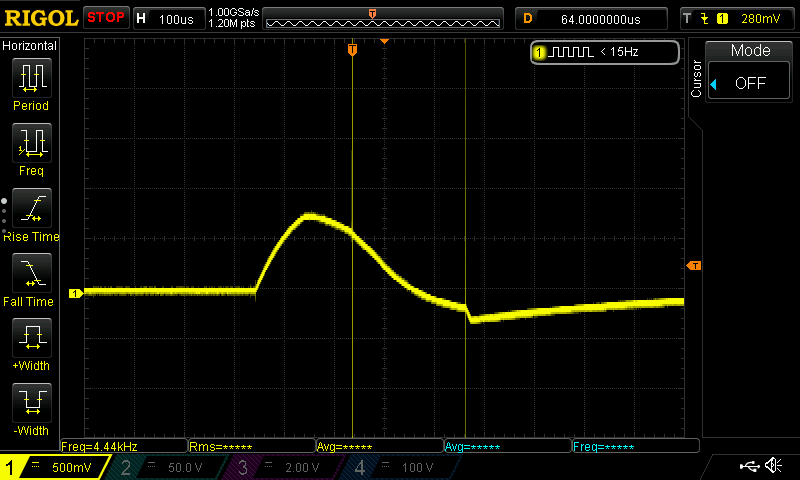
Current transformer, firing at 260 V burned out FETs: Current Transformer, firing at 260V burned out fets
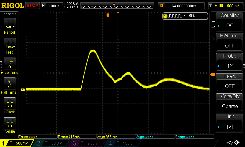
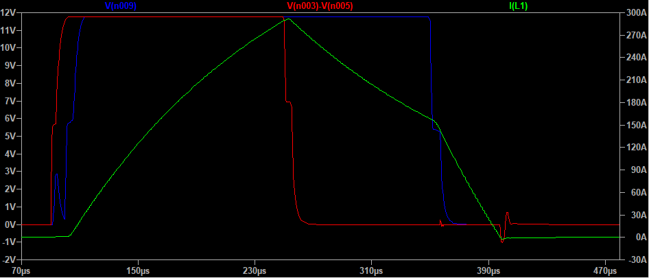
Current waveform from LTSpice: LTSpice Simulation

Datasheets:

MOSFETs FCH041N60F

Power diodes C6D10065E

Gate drivers MAX22702E

Addressing failure mode theories from my previous question:

  • Very fast current reversal in leads to cap bank may have lead to inductive voltage spike. [Added caps right at MOSFETs, slowed down switching, added TVS diodes]

  • Out of control ringing (not sure why that would cause a failure, but still not good). [Added a snubber to the coil. Sim showed this making a huge difference]

  • Core saturation leads to extremely high current. [checked with current transformer, no current spike.]

  • d(Vds)/dt exceeds mosfet rating and burns it out due to parasitic current paths. [Simulation shows ~90 V/us MOSFET rated for 100 V/ns]

  • Counterfeit parts. [Now using all parts from Digikey, no more ebay MOSFETs]

  • Coil capacitance leads to very brief high current spike. [Not visible on scope. Sim doesn't show any issue with a capacitance of 10 pF]

Summary:

I'm running out of ideas for what's causing the failure. My current best guess is some kind of high frequency resonance due to parasitics? That huge spike on the mosfet gate when switching to freewheeling seems like something, but I could just be noise? There is a 12 V TVS as close as it could possibly be to the gate and source.

Any theories would be appreciated. I'll test them if I can and report back.

\$\endgroup\$
2
  • \$\begingroup\$ What peak voltage do you measure across Q1 and Q2? What’s the stray inductance between C10 and your capacitor bank? \$\endgroup\$
    – winny
    Commented Feb 26, 2023 at 20:03
  • \$\begingroup\$ Between C10 and the cap bank is a twisted pair of 22awg wire approx 2cm, I estimated 34nH. I'm sorry I didn't measure the voltage at the drain of q1, I should have. Q2 is hard to measure. I can do it using math and 2 probes though. \$\endgroup\$
    – Drew
    Commented Feb 27, 2023 at 2:31

2 Answers 2

3
\$\begingroup\$

300 volts divided by 42 uH gives quite a high current growth rate about 7 A/us. In 150 us that means a high peak current, over 1000 amperes. Fets themselves probably limit it to a lower value as your simulation attempt suggests, but that means high Vds and high current at the same time. That's, of course, not based on measurements in your circuit, but fets do not live long when used out of their safe operating area. See the datasheet. There's mentioned the maximum allowed peak current limited by the die size and the safe operating area.

Check also what kind of load is caused by the high side driver power supply U1. Perhaps its minus output is not especially freely floating. Check if there's a substantial capacitance from the minus output of U1 to the ground. That's well possible if U1 is not specially designed for this purpose i.e. allowing with no harm one to kick it's output potential suddenly 300 volts upwards. Many power supplies have an intentionally added capacitor between it's input and output to reduce harmful radio noise emissions. If you have it, too, it may essentially short your high side fet. After it's melted the low side fet goes to the same route.

\$\endgroup\$
2
  • \$\begingroup\$ Thank you I will try to check both of those things. I didn't consider the capacitive coupling in U1. Granted, these supplies usually call for external caps to shunt EMI. \$\endgroup\$
    – Drew
    Commented Feb 27, 2023 at 2:37
  • \$\begingroup\$ I checked the high side power supply. It's specified to have a coupling capacitance of only 20pF. I also measured it with an LCR meter and got 30pf. At least on the SIM that doesn't seem to be enough to cause an issue. \$\endgroup\$
    – Drew
    Commented Apr 15, 2023 at 17:20
2
\$\begingroup\$

You're almost certainly operating outside of the MOSFET SOA. Based on ideal operation, you're right on the edge of what your MOSFETs can handle, with no real margin for non-ideal effects.

Your MOSFET gate driver circuit also looks problematic to me.

The C30/C31 capacitors should be removed. They have no positive effect here, will waste power in the gate driver, and will form a capacitive divider on the gates as they discharge which might lead to parasitic self-turn-on. You want less capacitance on the gate, not more. If you want to slow down the slew rate, use a higher gate resistance.

R2 and R4 don't do anything. Remove them.

Based on the trace in picture 2, you've got significant ringing on your gate, and might be exceeding \$V_{gs(max)}\$ - the scale isn't really clear to me. This can be reduced by increasing your gate drive resistance. Your current value of 10Ω is a little low anyway; based on a simplistic RC charge/discharge model you're achieving a rise time of around 130ns.

You aren't using asymmetric drive on your MOSFET. This leaves you vulnerable to the Miller self-turn-on effect while the MOSFET is being switched off. The MAX22702 also does not have an active Miller clamp like the MAX22701 does.

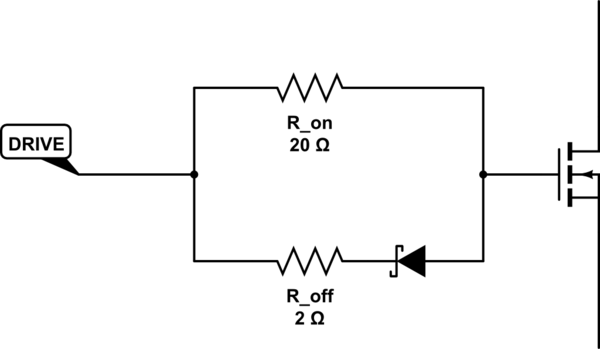
Typically you want your gate discharge current to be higher than your gate charge current, which can be achieved as shown in figure 17 of the MAX22702 datasheet. Essentially you have two gate resistors in parallel, with a diode in the reverse path:

schematic

simulate this circuit – Schematic created using CircuitLab

The resistor values are just examples.

Your driver is also optimised for SiC, so it has a faster rise time than you probably want with this regular silicon MOSFET, especially with the relatively massive gate capacitance of the FCH041N60F.

Given your application I'd consider swapping the MOSFETs out for SiC ones. Your driver is optimised for driving SiC MOSFETs anyway, and they're very good at withstanding high voltages.

\$\endgroup\$
11
  • \$\begingroup\$ Where do you think the ringing in the second picture is coming from? The spike occurs when the other mosfet switches off. Do you think it's the capacitance Cgd? That's why I included the 100nf caps gate to source, to act as a divider for Cgd. Also isn't the rise time more like 1-10uS, given the additional capacitance? \$\endgroup\$
    – Drew
    Commented Feb 27, 2023 at 2:44
  • \$\begingroup\$ The rise time was calculated based on you removing the caps. The gate capacitors are definitely not doing what you hope they are doing. They'll be charged up, but the loop inductances will cause all sorts of weird behaviours at the driver rise times, and they'll almost certainly cause big problems with self-turn-on. My guess is that your entire circuit is suffering from parasitic inductance, due in part to all the wired-together TH parts. I think the best approach here is to simplify things and take a step-by-step analytical approach rather than to keep trying to add extra protection tricks. \$\endgroup\$
    – Polynomial
    Commented Feb 27, 2023 at 3:19
  • \$\begingroup\$ Here's what I'd do: Remove the gate caps and the gate TVS diode. Remove the LEDs on the gate lines (they have junction capacitance!). Turn as much of the circuit as you can into a PCB and use SMD instead of TH wherever you can. Use asymmetric gate drive resistors. Dump the random assortment of 0.1uF/1uF/10uF decoupling networks - swap them for a single 10uF 0402 6.3V MLCC on <5V stuff, or a pair of 10uF 0603 25V MLCCs on 12V stuff, placed as physically close to the driver ICs as you can. Add a 220uF electrolytic somewhere in the vicinity for bulk decoupling. Use MOSFETs with more SOA overhead. \$\endgroup\$
    – Polynomial
    Commented Feb 27, 2023 at 3:25
  • \$\begingroup\$ Remove all of the protection and filtering stuff you've added. TVS diodes, C7, the ferrite bead, R1, etc. You don't necessarily have to remove the footprints from your PCB - if the part is in series, replace it with a 0R SMD resistor, if it's in parallel, mark it DNP. Simplify everything down to the basics, then start testing. Make sure each stage of the design works in isolation. Probe everything, systematically. Start with the HV line at just 10V or so. Check for noise on the signal lines and the power lines during switching transients. Only then start ramping the voltage back to 300V. \$\endgroup\$
    – Polynomial
    Commented Feb 27, 2023 at 3:41
  • \$\begingroup\$ I've already done most of that. If you take a look at my original design, you'll see it was all on a PCB and mostly SMT . It had no "protective" components, and the LED capacitance was shielded by a 1k resistor. I moved to the power component pack so that connecting legs could be directly soldered together right where they come out of the packages. Most of the connections are less than 2mm. I did this to minimize stray inductance. \$\endgroup\$
    – Drew
    Commented Feb 27, 2023 at 4:01

Your Answer

By clicking “Post Your Answer”, you agree to our terms of service and acknowledge you have read our privacy policy.

Not the answer you're looking for? Browse other questions tagged or ask your own question.