0
\$\begingroup\$

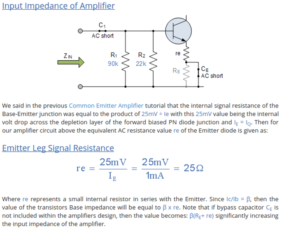
enter image description here

Why we need to consider the emitter resistance re while calculating input impedance of the given amplifier circuit? Is this a compulsion? I found out that even in case of common collector amplifier the emitter resistance is again included in the calculation of input impedance despite the fact that we are taking output across the emitter in common collector amplifier. And how can we derive base impedance = beta * re ?

\$\endgroup\$
5
  • 2
    \$\begingroup\$ It's only a compulsion if you want the amplifier to work correctly and/or to pass your course. The answers to your questions are contained in the material that you posted. Go though it slowly and be sure to understand what it says. Also, talk to other people studying the same material about what this text means - it's all there. \$\endgroup\$
    – Russell McMahon
    Commented Mar 3, 2015 at 15:09
  • \$\begingroup\$ What i am confused is that even in case of common collector amplifier the emitter resistance is calculated on input impedance side but not on output impedance side? \$\endgroup\$ Commented Mar 3, 2015 at 15:19
  • \$\begingroup\$ Think of base emitter junction as a real diode, which has a cut-in voltage and forward resistance. The forward res is calculated from diode eqn by differentiating it. \$\endgroup\$ Commented Mar 3, 2015 at 15:37
  • \$\begingroup\$ I think, differentiating the diode equation will give us a typical input resistance in the order of some kohms: 1/rbe=d(Ib)/d(Vbe). \$\endgroup\$
    – LvW
    Commented Mar 3, 2015 at 15:50
  • \$\begingroup\$ @LvW . Ic = Ico* (e^ (V / nVt)) gives the regular old exp Vt/Ic for resistance. And base input res is infact (B+1) times re. So it should come in Kohms I guess. \$\endgroup\$ Commented Mar 3, 2015 at 16:27

1 Answer 1

2
\$\begingroup\$

My recommendation: Forget the link which gaves you the above information, which is false resp. misleading. (By the way: This link leads you to other "explanations" which also are wrong). Hence, you should not blindly trust any information available in the internet.

The text says that the "25 mV value being the internal voltage drop across the depletion layer of the forward biased pn diode junction". That`s pure nonsense.

This value of 25 mV is the so-called "temperature voltage VT" which depends on the environment temperature and appears in the exponent of the e-function describing the relation between the controlling base-emitter voltage and the emitter current.

And what about the "resistance" re, which appears in the above figure outside the transistor?. In fact, it is NOT a resistance - it is the inverse of the transconductance gm=1/re - and some people prefer the use of re instead of gm. Note that the transconductance gm=d(Ic)/d(Vbe) is nothing else than the SLOPE of the transfer curve Ic=f(Vbe) - measured in the selected DC operating point.

More than that, it can be easily shown that the slope d(Ic)/d(Vbe) is identical to gm=Ic/Vt (VT: temp. voltage); this gives you the relation between gm=1/re and VT.

Hence, gm is the most important parameter which determines gain. It relates input voltage and output current (therefore, it is called "mutual" transconductance gm). This can be seen in the known gain formulas (common emitter):

(a) without feedback: Gain=-gm*Rc
(b) With feedback (emitter resistor Re): Gain=-gmRc/(1+gmRe)

(Sometimes you can read: (a) -Rc/re and (b)-Rc/(Re+re) ).

EDIT: Differential input resistance at the base node (without feedback resistor Re):

The input characteristic of the BJT is also exponential with the slope

1/rbe=d(Ib)/d(Vbe)=(1/beta)[d(Ic)/d(Vbe)]=gm/beta.

Hence: rbe=beta/gm (or: rbe=beta*re).

Final comment: I think, this post is a typical example for the confusion which can be caused by using such "artificial" terms like re which have no physical meaning.
\$\endgroup\$
3
  • \$\begingroup\$ You have provided some very useful information which better explains the situation. However, I think the OP will find it very confusing as it looks like their level of experience is not enough to understand the material that you have provided. || Interest only: I tell people that a "rule of thumb" is that the maximum gain of a common emitter silicon bipolar transistor is ~= 38.4 x Vload, and people think it sounds crazy :-). It's not. I can see that you could derive that "rule of thumb" if you do not know it already. \$\endgroup\$
    – Russell McMahon
    Commented Mar 3, 2015 at 20:27
  • \$\begingroup\$ Russell, I didn`t know this "rule of thumb". I will try to justify - I suppose it has to do with the following effect: Each attempt to have more gain by increasing Ic (and, hence, the transconductance gm) causes an increased DC drop across Rc, which - in turn - requires Rc reduction (to keep the bias point). Right? Thank you. \$\endgroup\$
    – LvW
    Commented Mar 4, 2015 at 9:10
  • \$\begingroup\$ More or less yes. Cheating :-) - Supply 1 mA to a common emitter BJT with a 1k load resistor and say >= 15V supply (could be lower here). What is Re?. What is gain? Change to 2 mA. Now 10 mA. What happens. What is Vload and gain. And Gain/Vload. Once you see it it all is obvious. In the OP's example I'd use Re = 26/mA. I suspect the 25 he uses is a nice round figure for students. \$\endgroup\$
    – Russell McMahon
    Commented Mar 4, 2015 at 12:31

Your Answer

By clicking “Post Your Answer”, you agree to our terms of service and acknowledge you have read our privacy policy.

Not the answer you're looking for? Browse other questions tagged or ask your own question.