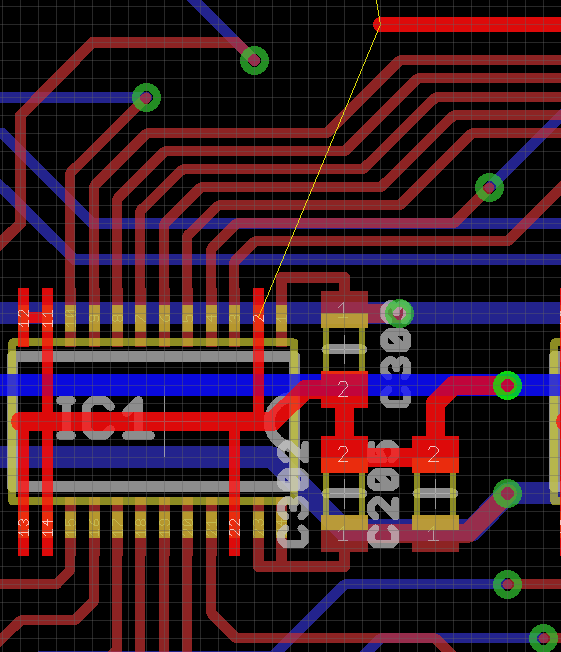
Previously I've been using ground plane pours in Eagle to connect ground points and also to surround lines that I feel need protecting from surrounding noise. This is on two layer boards. By drawing a GND poly around the dimension layer on top and bottom you can connect all GND points without thinking too much. Less etching is a plus too, even if you end up with planes that are islands (I'd normally via those to a bottom ground plane)
Olin and others indicate it's a bad idea to do this. Thus I've been localising my ground planes:

The above image has GND highlighted and I haven't done the local ground plane pour around IC1 yet (on top or bottom). This is a '245 level shifter from 1.8V to 3.3V. As per Olin's post, I have GND local and then viaed to the bottom ground plane at one point after a decoupling cap.
Most of the bus lines coming off are SPI at 10MHz and GPIO lines. The GND line at the top is a "protection" line - like crystal guard ring - between SPI CLK and I2C lines above it. It's supposed to indicate where I'd pour a ground shield.
I don't know where to connect that ring though. Not to the local IC1 ground plane surely, even though it's part of IC1 signal outputs?
As my bottom GND pour will be one single plane, should I presume any top shield pouring can connect to the bottom pour at various points?
I'd like to know how to do it properly as doing a poly GND around the dimension line in Eagle causes the shield ground pour to connect all the other ground pours which is not what I want at all. Should I use what Olin called "shorts" between GND and SGND (shield ground) and then do an SGND poly pour?
