2
\$\begingroup\$

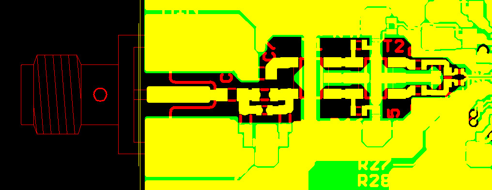
Using a snapshot of an eval board design below as an example, voids are added to the ground plane on layer 2 (green) right underneath the analog signal path on layer 1 (yellow). This causes the analog traces to reference the ground plane on layer 3 instead. I understand that this increases trace width, hence improved impedance matching and decreased signal loss at the trace-to-pad junctions.

What is the best way to determine the minimum width of the voids that guarantees that the signals do not reference layer 2? I assume this is based on the trace widths and the layer separations.

enter image description here

\$\endgroup\$

1 Answer 1

3
\$\begingroup\$

The "best" way is to build a board and measure the impedance. Another "best" way is to simulate it with some form of EM simulation software. The "quick" way is to use a rule of thumb like 5 tracewidths on either side (for microstrip). So, if your trace is 10 mils, keep all copper on layer 2 at 50 mils or more away.

However, that looks more like coplanar waveguide than microstrip...

\$\endgroup\$
1
  • 2
    \$\begingroup\$ The board thickness matters here too, copper on layer 2 should be relieved at least a couple of board thicknesses away from the signal trace. I would say the real way is to simulate -- simply measuring the impedance won't easily tell you what fraction of the return current is in layer 2 vs 3. So you should simulate to get the gap size, then measure the impedance and adjust the track width to hit your target. \$\endgroup\$
    – Evan
    Commented Jul 25, 2016 at 19:39

Your Answer

By clicking “Post Your Answer”, you agree to our terms of service and acknowledge you have read our privacy policy.

Not the answer you're looking for? Browse other questions tagged or ask your own question.