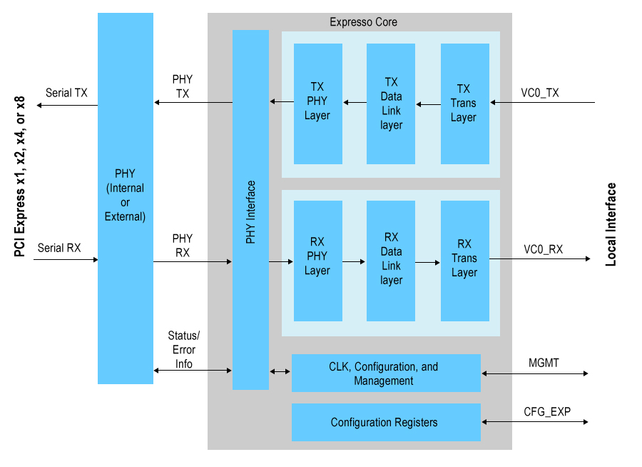
Much of what goes on in PCI Express is 'under the hood' in a PCI express endpoint core; that includes the link partner link-up (using the LTSSM), receiving and transmitting TLPs and DLLPs and whatever else is required to actually move data around in the link.
You may find this picture useful (source)

The really fast wire speed stuff (up to 8Gb/sec for gen 3) is handled by a SERDES and on the internal side the data rate is much slower on a per bit basis (the data are now parallel).
In your case, the FPGA logical core (which is utilising whatever is being transported) has no datalink processing overhead; the entire
TLP is handed over from / to the logical core from the PCI express endpoint implementation.
As such, the processor itself has little overhead using PCI Express.
In PCI Express (as in Infiniband) independent local clocks may be used (which is the raison d'etre for the SKIP ordered set [extensive description]) because the link is source synchronous (i.e. the clock is embedded in the data on the wire).
Most middle range processors and controllers integrate a PCI express interface even though they may not be capable of filling the pipe (250 MBytes/sec for gen 1, 500 MBytes for Gen 2) simply because the interface is ubiquitous. PCI express does require a 100MHz clock, though, so you are unlikely to find one of these on a really slow device.
Gaming machines may have a 16 lane Gen 3 link with a throughput of 15.754 GBytes / second (peak) which is likely to need a pretty high end device at both ends of the link simply due to the data rate.
As the PCI Express endpoint is actually doing all the grunt work of building DLLPs and TLPs, the processing requirement at the interface to the PCIe block is limited because the majority of PCI express (just as with PCI) are memory transactions; it looks just like a memory read or write.
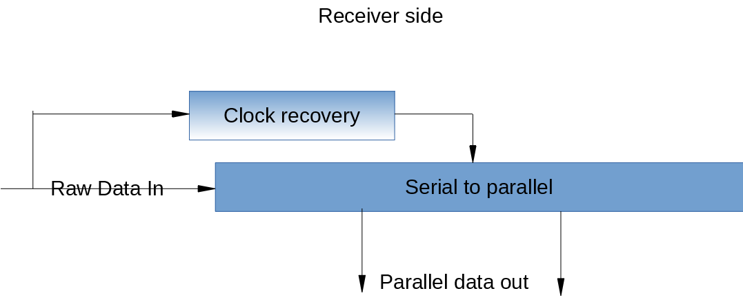
This is an incredibly wide subject, so I will start with part of the physical layer at the receiver (highly simplified).

This is where the really high speed stuff is done; this block receives the raw data on the wire into what is in reality a shift register although the specific implementation may be quite clever with things such as multi-phase clocks, but the basic principle is a shift register.
The clock recovery circuit does precisely that; recovers the transmitter clock from the received data. I mentioned above the fact that this is a source synchronous link.
Xilinx implements the high speed register (and significant control logic) using their GTX transceivers, which are what are used when implementing the PCI express hard endpoints available in many of their devices.
An elastic buffer is used where the source clock domain and destination clock domain are not generated from the same master oscillator. As no two oscillators are precisely the same, this is a necessary item in a PCI express link with separate clocks at transmitter and receiver.
If a transmitter is sending data slightly faster than the receiver can handle, without some control we would end up with a buffer overrun; to deal with that the link sends a SKIP ordered set; this data set is literally thrown away - it never ends up in the receiver payload FIFO.
If you are getting the impression that this is a very broad subject (you should), then look around for the architecture overviews and ask specific questions on each part of the architecture; I cannot possibly do justice to the entire subject in a single answer.


