2
\$\begingroup\$

enter image description here

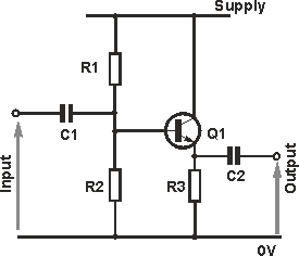
I'm in the need of a buffering circuit for a project and I would like to use a common collector amplifier or emitter follower for this purpose. Above is a schematics of the circuit I'm looking into.

However, I'm having slight trouble understanding this circuit, specifically why the voltage at the output is the input voltage minus the base-emitter voltage drop (around 0.7 volts). Doesn't the capacitor C1 cause a voltage drop? It has capacitance, therefore it has impedance. If this circuit is used as a unity-gain current amplifier (buffer), I want only a small amount of current to enter at the input. Therefore, C1 should be quite small capacitance (because current is the voltage divided by the impedance, which in turn is inversely proportional to the capacitance). But if it has large impedance, I think it would have a larger voltage drop across it, and the output voltage would be input voltage minus the capacitor drop minus the diode voltage drop.

Somehow I think I'm thinking about this circularly, and I can't really make sense of what's happening. Can somebody explain to me why the output voltage is (almost) the same value as the input, and how the capacitor values are chosen?

EDIT: What if there is a load across the output? Say, a small-ish resistor. If the input capacitor is also small impedance, would there now be a quite large current through the circuit from input to output, defeating the whole purpose of the buffer?

\$\endgroup\$
7
  • \$\begingroup\$ Please notice that the BJT is already prophetly biased. So, the DC voltage at the base is 5.6V for a example, hence the emitter DC voltage will be Vbe smaller (around 0.6V), so we will have a 5V DC voltage at the emitter. And now any change in the input voltage "will appear" at the base as Vdc+Vac thanks to C1 capacitor. So, now if the voltage at the base change from 5.6V into 5.6V (1V change) the emitter voltage will follow this change. And the emitter voltage will change from 5V to 6V. \$\endgroup\$
    – G36
    Commented Jul 13, 2017 at 21:13
  • \$\begingroup\$ electronics.stackexchange.com/questions/310471/… \$\endgroup\$
    – G36
    Commented Jul 13, 2017 at 21:13
  • \$\begingroup\$ Your intuition is correct the impedance of the capacitors need to be lower than the effective resistance around them for your signals of interest. C1 and C2 both form High-pass filters. The design goal is make to corner frequency of the HPF low enough for you signals of interest to pass. \$\endgroup\$
    – sstobbe
    Commented Jul 13, 2017 at 21:30
  • \$\begingroup\$ Your desired load is important to know. The emitter follower BJT can source current but it cannot sink it. That will be the job of \$R_3\$. So it's not going to push-pull, symmetrically. \$\endgroup\$
    – jonk
    Commented Jul 13, 2017 at 22:45
  • 1
    \$\begingroup\$ @Circuitfantasist I was speaking at the time about its ability to act as push-pull. It's not at all symmetric. Which is why the load is important to know about and why I asked about it. \$\endgroup\$
    – jonk
    Commented May 16, 2020 at 19:27

2 Answers 2

0
\$\begingroup\$

You have shown an AC amplifier. The average input current is essentially zero, and the average voltage is whatever your load drags it to. The emitter of the transistor sits at roughly \$V_{Supply} \cdot \frac{R2}{R1+R2} -0.7V\$ if R3 isn't too low value, but that emitter voltage does not make its way to the output except momentarily when power is applied.

The input impedance should be about R1||R2 for frequencies in which the amplifier is useful, that's ignoring the series impedance of the capacitor and the loading of the base, both of which should have much less effect than R1||R2.

\$\endgroup\$
3
  • \$\begingroup\$ But if the input impedance is the parallel combination of R1 and R2, would that imply that no current flows through the base-emitter junction? Let's say there is a quite small resistor across the output. Then as both the input capacitor and the output load are small impedances, there should be quite a big current from the input to the output, defeating the purpose of using a buffer. What am I missing here? \$\endgroup\$
    – S. Rotos
    Commented Jul 13, 2017 at 19:41
  • \$\begingroup\$ @S.Rotos what you are missing is that the circuit is high impedance in the input and relatively low impedance on the output. Basically, it will act as a buffer with unity gain in the required frequency range if the resistor and capacitor values are chosen correctly. \$\endgroup\$
    – Trevor_G
    Commented Jul 13, 2017 at 20:23
  • \$\begingroup\$ There is current into the base, but it is generally small, because of the current gain of the transistor. This circuit has no voltage gain, but it can have current gain. If the load ||R3 is 1K then the impedance looking into base might be 300K. If R1&R2 are 20K then the impedance at frequencies of interest is 10K||300K = 9.7K or ~10K and the amplifier has a current gain of about 10. \$\endgroup\$ Commented Jul 14, 2017 at 9:30
0
\$\begingroup\$

C1 is used to superimpose your signal on top of the base bias voltage. C2 acts as a dc blocking component which blocks the DC component of the emitter voltage and lets through the buffered signal. C1 in connection with R1||R2||(Input impedance of the transistor) forms a high pass filter.

Neglecting C2 for now here's how you should pick up a value for capacitor C1. The input impedance of an emitter follower is BetaRE, where Beta is the current gain of the transistor, and RE the resistance measured across the emitter and ground. As I said, C1 together with R1||R2||BetaRE forms a high pass filter. If Beta*RE is large compared to R1||R2 then you can write simply

$$H(w)=\frac{R_1||R_2}{R_1||R_2+1/jwC_1}$$

where its absolute can be written as

$$|H(w)|=\frac{R1||R2 \times wC_1}{\sqrt(1+R_1||R_2 \times wC_1)}$$

Now if you want to pass all signals of interest then you should choose C1 so that

$$C1 >\frac{1}{2\pi f R_1||R_2},$$

where f is the frequency of the signal of interest. For example, for R1=10k, R2=110k, RE=100k, and f=400Hz, you'll need to set C1 equal to 0.1uF or so.

\$\endgroup\$

Your Answer

By clicking “Post Your Answer”, you agree to our terms of service and acknowledge you have read our privacy policy.

Not the answer you're looking for? Browse other questions tagged or ask your own question.