30
\$\begingroup\$

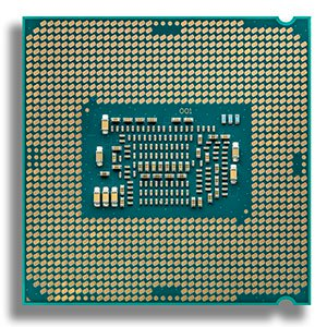
The transistory bits of an integrated circuit are approximately in the centre of the (plastic or ceramic) package. They sometimes get hot, and we cool them by affixing a heat sink to one side. Sometimes we just blow air over them with a fan. Some of this heat propagates upwards, but some must also go downwards towards the PCB. I don't know the ratio. The following is the underside of a Intel Core i7-7700K CPU dissipating 91W of heat:-

cpu underside

There are many connection pads. Clearly they act as lots of micro heat sinks that transfer some significant proportion of the heat to the socket /PCB. Indeed many surface mounted components dissipate heat through (via stitched) copper layers.

So if cooling is important (as for the CPU overclocking community), why aren't CPUs cooled from beneath the PCB as well, with say a fan?

EDIT:

Whilst the below comments are on the whole negative, there are two new items. One, there is a long thread on Overclock suggesting that a significant number of degrees could be taken off the CPU temperature with a fan on the backplate. And two, I tried it (admittedly with only a Raspberry Pi). I covered the top side with cloth to isolate the Broadcom CPU, whilst cooling the underside only with a 60mm fan. The fan reduced the maxed out CPU temperature from 82 deg. to 49. Not bad, so I think that this idea has legs...

\$\endgroup\$
13
  • 26
    \$\begingroup\$ Because of an annoying thing called a ZIF socket and a PCB that gets in the way \$\endgroup\$
    – user16222
    Commented Jan 15, 2018 at 22:53
  • 6
    \$\begingroup\$ It was a facetious reply :) the pins are actually quite efficient are drawing heat away. Likewise the ground plane helps \$\endgroup\$
    – user16222
    Commented Jan 15, 2018 at 22:59
  • 3
    \$\begingroup\$ It's just not practical. To do this you need to dig one hole on the CPU PCB and another on the main board PCB. Even back in the days when CPU die is on the underside of the package no one choose to dig a hole on the main board. \$\endgroup\$ Commented Jan 16, 2018 at 1:01
  • 14
    \$\begingroup\$ Google “flip chip”. Most modern processor chips are mounted upside down so the actual silicon chip is closest to the top of the package. This makes top-side heat sinking very effective. \$\endgroup\$
    – DoxyLover
    Commented Jan 16, 2018 at 4:03
  • 2
    \$\begingroup\$ The PCB around the CPU socket is busy dissipating heat from the voltage regulator components - it could conceivably be advantageous to have the CPU thermally isolated from the motherboard. \$\endgroup\$ Commented Jan 16, 2018 at 11:24

7 Answers 7

37
\$\begingroup\$

They aren't cooled from below because they have pins on the bottom, and FR4 below that.

Due to having a much lower thermal conductivity, $$ \begin{array}{rrl} \text{Copper:} & 385\phantom{.25} & \frac{\mathrm{W}}{\mathrm{m}{\cdot}\mathrm{K}} \\ \text{Aluminum:} & 205\phantom{.25} & \frac{\mathrm{W}}{\mathrm{m}{\cdot}\mathrm{K}} \\ \text{FR4:} & 0.25 & \frac{\mathrm{W}}{\mathrm{m}{\cdot}\mathrm{K}} \\ \end{array} $$the material on the bottom of the CPU would transport much less heat.

Odds are you wouldn't want to surround the signals with metal which would change the impedance drastically, so metal on the bottom is more of an issue. If you did build a socket out of metal, it would need to be micromachined, which would be many times more expensive than a plastic injection molded socket. These things would prevent you building a processor socket that would wick heat away.

You could put a cooling block on the bottom of the board, but the PCB material (FR4) would reduce the cooling substantially.

\$\endgroup\$
2
  • 4
    \$\begingroup\$ But the FR4 figure is misleading somewhat. The PCB beneath a modern CPU is highly populated with many solder filled vias and copper tracks. Look at the pin density on my photo. And the ground /power planes. And through board socket and cooler mounts. I would expect the aggregate thermal conductivity of all of that to be much higher than 0.25. Just stick your finger under your motherboard to feel the heat... \$\endgroup\$
    – Paul Uszak
    Commented Jan 16, 2018 at 21:39
  • 1
    \$\begingroup\$ I agree that it would be higher than .25, but those vias are not very large and nowadays they run microvias and blind and buried vias so most of that copper does not run all the way through the board. Any copper will wick away heat, but you also need a large thermal pathway which isn't going to happen on the bottom of the CPU, because it is much easier to place it on the top. \$\endgroup\$
    – Voltage Spike
    Commented Jan 16, 2018 at 21:54
22
\$\begingroup\$

Cooling isn't important, it's crucial. A modern CPU can easily put out something between 15 W and 200 W, from a die that's a few cm². If you're not transporting that heat away, that chip has to stop operating, slow down, or: just burn up.

With that out the way: Where do you put your heat from there? The cooling surface of a motherboard is very limited compared to the surface of a CPU cooler's body. The heat transport capability of the copper layers isn't bad per se, but compared to a massive block of copper and aluminium (and, often, convectional heat piping), it's negligible.

Then: The motherboard itself often isn't the coolest place, especially around the CPU. There, the whole power supply chain of the CPU is situated. That has a good efficiency, but with a load of several dozen amperes and rapidly changing load scenarios, it's no wonder these converters get hot, too.

I'm certain that in custom High Performance Computing and military builds you'll find specialized CPU packages that give underside access to parts of the CPU, but in socketed mainstream CPUs, that's just not possible mechanically nor thermally overly advantageous.

Note that this doesn't apply to all CPUs. If you go into the embedded sector, you'll often find smaller CPUs with a heat-sinking pad in the middle. It just doesn't seem feasible for larger CPUs.

I'm certain Intel and AMD wouldn't put these passives on the bottom of their CPUs if they could avoid it. In fact, look at that picture: the green board you're looking at is not the die, it's the PCB carrier that the board is connected to; that's the technological price you pay for being able to cheaply mass-produce interchangeable CPUs rather than just having motherboards with the CPUs Chip-scale-package ball soldered onto them directly – and you can't completely have that, even theoretically, because the heat from that CPU is just so much that a heat spreading metal plane has to be pressure-fit on top of it, and you can effectively only do mechanically that by having the die on some sort of substrate.

\$\endgroup\$
1
  • 10
    \$\begingroup\$ Further reading: the "power wall": why we can't build CPUs that dissipate more than about 200W, even if we wanted to. TL:DR: power density with tiny transistors is a problem. (That article has a nice overview of CPU microarchitecture from early pipelined CPUs up to modern OoO, as well as the power wall issue that caused Pentium 4 to fall flat on its face. Intel picked the wrong time to switch to a power-hungry speed-demon design, just a couple generations before the transistors were small enough for that to be the limiting factor.) \$\endgroup\$ Commented Jan 16, 2018 at 10:13
12
\$\begingroup\$

A response that hasn't been given yet is because of the way they are built. CPUs used in computers and laptops are (at least to my knowledge) never a full flip-chip. They simply have too much connections to allow easy flip-chip on a simple PCB process used on motherboards. I mean simple here compared to the processes needed for RF/millimeter wave applications, or a process that allows densities where you really can fan out 1000+ pins on a few square millimeters.

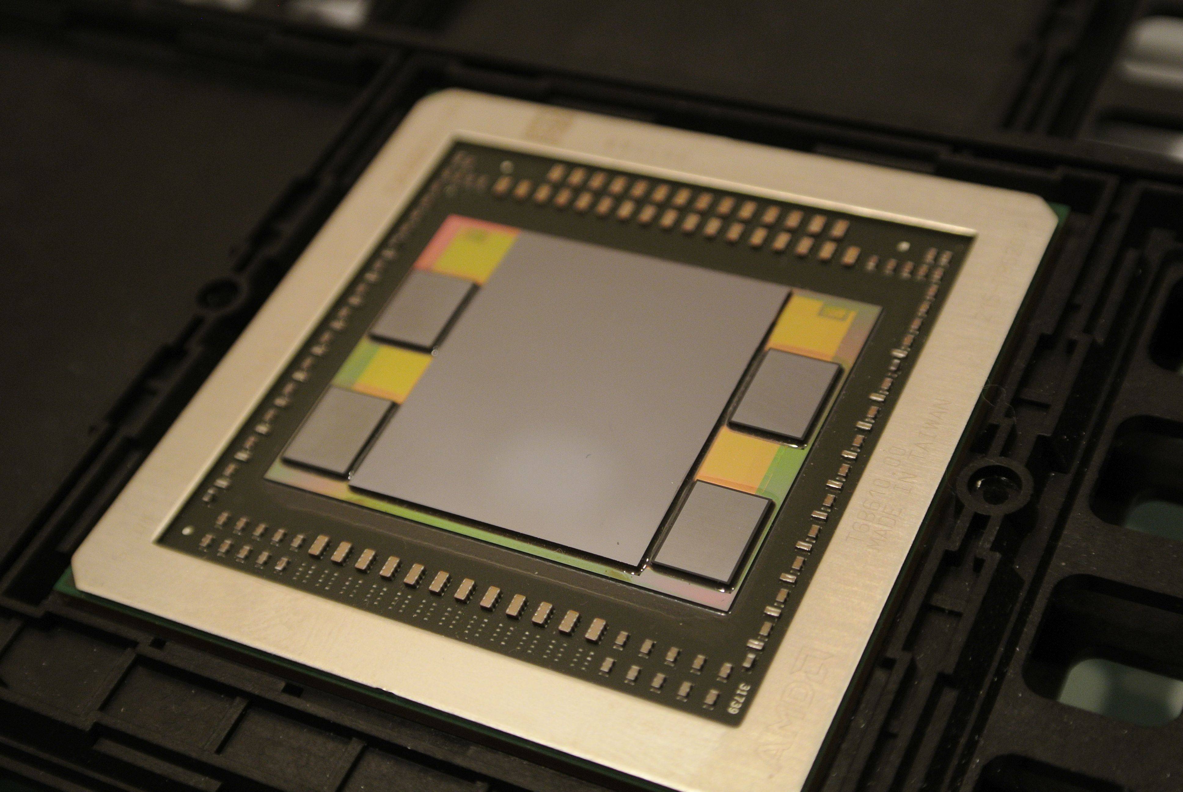
For this reason, CPU dies are always flip-chipped onto a interposer. This is often ceramic, and made out of many layers. Here is an example, from wikipedia. Yo can see 5 separate dies on this package, in addition to a large amount of small passives around the edges (from what I can tell this is actually a even more complex stack-up, with a silicon interposer to interconnect the different dies, and that is then put on top of a ceramic interposer).

enter image description here

Why does this all matter? You suggest that you must be able to efficiently transfer the heat through the pins on the CPU. However, this is not the case, because of this interposer. This is not like a big power device where the big metal bit is actually connected to the silicon - there is a lot of stuff in between.

As a result the thermal conductivity from the die to the pins is still low - so even if you were to find some very nifty way of getting all the heat away from those pins, you would barely see any improvement, since you will still be dealing with order-of-magnitude greater thermal resistance compared to a metal heat-spreader that is in direct contact with the top of the silicon.

If you go to CPUs used in phones or embedded devices, which a "bottom heatsink" pad, things are different. Here they don't use a flip-chip approach. In the center of the BGA, they will have a metal place on which the die is thermally attached (this is usually also ground). They then use bondwires to connect up all the pins, still using a form of interposer with the metal in the middle (or the center metal is just a bunch of vias straight through to get low thermal conductivity). This means that there is a lot less material between that center cooling pad and the BGA pins, allowing for far more efficient heat transfer.

\$\endgroup\$
5
  • \$\begingroup\$ I think you got your wording backwards here: "the thermal conductivity from the die to the pins is still high", but it looks like you meant to say conductivity=low or resistance (resistivity?)=high, not high conductivity. \$\endgroup\$ Commented Jan 16, 2018 at 10:18
  • \$\begingroup\$ @PeterCordes Correct! Thanks for pointing that out, I'll correct it right away. \$\endgroup\$
    – Joren Vaes
    Commented Jan 16, 2018 at 10:22
  • \$\begingroup\$ Also, you need to put these capacitors somewhere, and it is crucial the connections are short. \$\endgroup\$ Commented Jan 16, 2018 at 15:52
  • 1
    \$\begingroup\$ Note that the image is of AMD's Fiji GPU, used in the R9 Fury series. The silicon interposer it uses is a rarity, even among multi-chip packages. Most simply put all the chips on the FR4 substrate, but Fiji's four stacks of High Bandwidth Memory required silicon to provide the necessary wire density for a 1024 bit bus to each stack. \$\endgroup\$
    – 8bittree
    Commented Jan 16, 2018 at 18:27
  • \$\begingroup\$ Re. last para. If the enclosure allowed it, could you then cool one of your bottom heatsinked chips from above as well, ie. both sides? \$\endgroup\$
    – Paul Uszak
    Commented Jan 17, 2018 at 21:37
12
\$\begingroup\$

Some of this heat propagates upwards, but some must also go downwards towards the PCB. I don't know the ratio.

That's true, heat propagates in all directions. Unfortunately, the rate of propagation (also known to be characterized as thermal resistance) is very different.

A CPU must be connected with peripherals/memory somehow, so it has 1000 - 2000 pins for that purpose. So the electrical path (fanout) must be provided, which is done via printed circuit board technology. Unfortunately, even if impregnated with bunch of copper wires/layers, the whole PCB thing doesn't conduct heat very well. But this is unavoidable - you need connections.

Early CPUs (i386-i486) were cooled mostly via PCB path, in early 90-th the PC CPUs had no heat sink on top. Many chips with traditional wire-bond mounting (silicon chip on the bottom, pads connected with wires from top pads to lead frame) may have thermal slug on the bottom, because this is the path of least thermal resistance.

Then the flip-chip packaging technology was invented, so the die is on the top of package, upside-down, and all electrical connection is done via electrically conductive bumps on the bottom. So the path of least resistance is now going through the top of processors. That's where all extra tricks are used, to spread the heat from relatively small die (1 sq.sm) to bigger heat sink, etc.

Fortunately, CPU design teams include sizable engineering departments who conduct thermal modeling of the CPU die and entire packaging. The initial data came from digital design, and then expensive 3-D solvers give overall picture of heat distribution and fluxes. The modeling obviously includes thermal models of CPU sockets/pins and mainboards. I would suggest to trust them with solutions they provide, they know their business. Apparently some extra cooling from the bottom of PCB just isn't worth extra effort.

ADDITION: Here is a lump model of a FBGA chip, which can give an idea to, say, LGA2011 Intel thermal model.
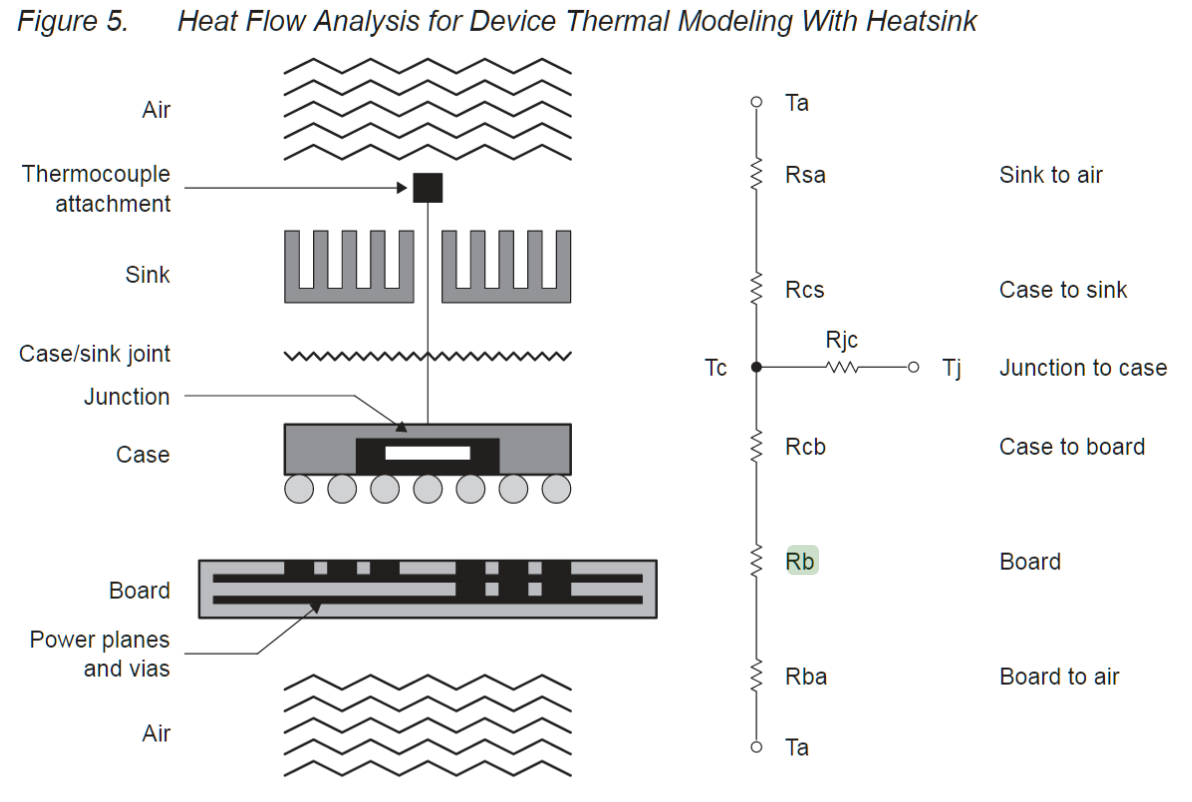
enter image description here

While the multi-layer PCB with thermal vias and 25% copper content might have somewhat good thermal performance, modern/practical LGA2011 system has one important element, a socket. The socket has a needle-type spring contacts under each pad. It is quite obvious that the total bulk of metal contact across the socket is quite smaller than the bulk copper slug on the top of CPU. I would say it is no more than 1/100 of the slug area, likely much less. Therefore it must be obvious that the thermal resistance of LGA2011 socket is at least 100X of the top direction, or no more than 1% of heat can go down. I guess for this reason Intel thermal guides totally ignore the bottom thermal path, it is not mentioned.

\$\endgroup\$
2
  • 3
    \$\begingroup\$ FYI, AMD's Epyc and Threadripper CPUs have pushed the maximum number of pins in a mainstreamish CPU from ~2000 to ~4000. Intel's current top end Xeon/Phi chips have used an ~3600 pin socket for longer but as a multisocket only platform are considerably more niche. \$\endgroup\$ Commented Jan 16, 2018 at 16:06
  • 2
    \$\begingroup\$ A very good review, but let me put you under some pressure now... What would you estimate as the split between heat going up and heat going down? This ratio is what led me to pose the question. \$\endgroup\$
    – Paul Uszak
    Commented Jan 16, 2018 at 21:30
2
\$\begingroup\$

In avionics, cooling is evaluated for all possible paths, including via the PCB.

A mainstream microprocessor in a laptop / desktop generally uses a mixture of conduction (heat sink) and convection (forced air usually) cooling. As the mixture of these two moves the majority of the heat away, the cooling mechanism via the PCB is sometimes ignored, but it is still present.

If equipment is in an unpressurised avionics bay, convection cooling rather loses meaning (the air density is very low meaning that there are insufficient molecules at high altitude to spread the heat). For that reason, conduction cooling is very widely used as it is the only truly effective cooling method in this scenario.

For this to be effective, numerous planes are used within the PCB as heat spreaders.

Where heat sinks are used (not a preferred solution but sometimes unavoidable), the path is still conduction cooled via heat ladders to a cold wall (this is a relative term - the cold wall may be at 70C or more).

Forced air is sometimes used, but within a pressurised chamber attached to the cold plate.

So in this scenario, cooling via all paths is utilised; conduction from both sides, FR-4 may not be particularly thermally conductive, but the copper planes are.

I went into a somewhat detailed thermal discussion in an answer to this question.

\$\endgroup\$
2
\$\begingroup\$

The actual answer is basic engineering. It is a lot easier to optimize a system if you can separate it into subsystems that can be independently optimized.

By optimizing one side for the connectivity, and the other side for heat removal. You have simplified the problem, while imposing, at most, a 2:1 penalty to either problem. Clearly, if you had much more heat than connections, or more connections than heat, this choice should be revisited, but that clearly is not the case.

This does not mean that it is not possible to remove heat from the underside, or to place connections on top, but at what cost? What other compromises must then be made?

Liquid-cooled cpu modules, while they are making a comeback, were rather common 30 yrs ago. When mainframes had cpu “envelopes” that were fully liquid-immersed, and thus removed heat from all sides of the enclosed ICs. This clearly presents a downside to the design of the connections, debugging, rework, and the types of liquid that can be used. Those are a lot of additional constraints to either subsystem. The fact that such choice was made, indicates that heat removal was the primary constraint.

Modern liquid-cooled supercomputers, have highly-optimized water micro-conduits on top of the wafer. While all of the connections are on the underside. Each subsystem is independent of the other, greatly optimizing the whole design.

In applications where the side opposite the connections is otherwise occupied, e.g., LEDs, lasers, optical links, RF ports, etc. the underside is the primary heat-removal path. And specialized substrates, with high heat conductivity, are generally used.

\$\endgroup\$
1
\$\begingroup\$

Though this topic was active years ago, I'm posting to help those who search afterwards. The comments giving reasons not to cool the underside of a heat source is non-nonsensical. The PCB is decent insulator slowing the heat transfer but itself will still get HOT just SLOWER than bare metal which conducts heat FASTER. The CPU is still a heat source so the heat will soak through even if slowly to the other side of the board. In addition as some have said, circuitry often extends to the underside which facilitates heat transfer through the PCB. Even more, board designer know management of heat sources is to pierce the PCB or purposely design areas where there are channels of lessor PCB insulation material sandwiched layers. Even if you don't believe any of this or perhaps your board is a special case, the easiest way to tell if you have a problem or not EMPIRICALLY is to use an infrared thermometer on the backside of the board and apply intake or exhaust to alleviate if the temperatures are high.

\$\endgroup\$

Your Answer

By clicking “Post Your Answer”, you agree to our terms of service and acknowledge you have read our privacy policy.

Not the answer you're looking for? Browse other questions tagged or ask your own question.