1
\$\begingroup\$

I am doing net-tie method to separate two different Ground Planes (for noise mitigation purpose), one ground plane is for RF circuitry and MCU, the other ground plane is for power and motor switching. I wonder if this is a good way of laying out net-tie

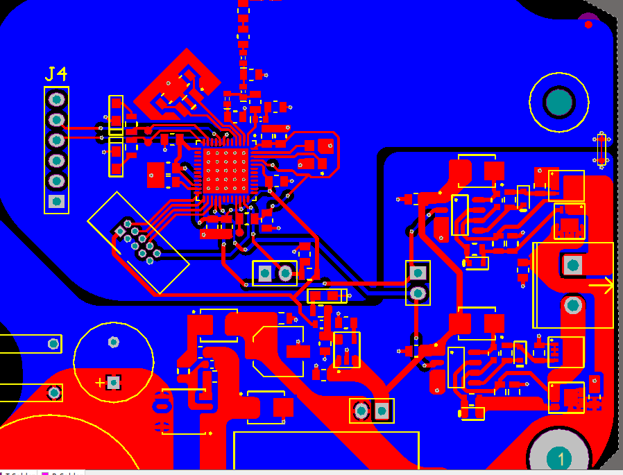
enter image description here

Here is the preview of the circuit, the net tie is laid at the top right hand corner, far away from power source. It stay on the top layer and I use via to tie to the ground planes that are mostly at the bottom layer.

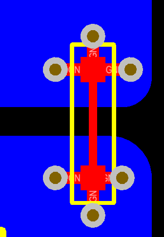
Here is the closer look at the net

Closer look of net tie

Please let me know if this method works.

Thanks.

\$\endgroup\$
2
  • \$\begingroup\$ Could you put some dimensions on those vias and traces? \$\endgroup\$
    – Voltage Spike
    Commented Jun 29, 2018 at 19:50
  • \$\begingroup\$ @laptop2d Hello, The width of net-tie trace is 0.2mm while the diameter of the via is 0.6mm and the hole size is 0.3mm, The trace width coming out of the pads to the vias is 0.3mm. Thank you for taking a look! \$\endgroup\$
    – AlexT
    Commented Jun 29, 2018 at 20:01

2 Answers 2

2
\$\begingroup\$

Yes that works if all you are doing is tieing the ground planes together. You are also creating an inductor with about 0.1nH and 7mΩ for the copper trace and roughly 0.3nH and 0.1mΩ for the vias on one side (for only three vias).

What doesn't make sens to me is why the vias are paralleled and then the trace is necked down to what I'd estimate somewhere in the range of 10 to 14mils. The resistance of the trace is much higher than the paralleled vias.

The other thing is your creating a long path for any return currents to get back to the processor by placing the net tie so far away from the other traces. The ground planes are separated with inductance and it doesn't look like you have a lot traces that crossover. If any of these are high speed (more than 20Mhz) the net tie will create problems.

Separating the ground planes with a net tie such as this creates a dipole antenna, which could create problems if you need to pass the limits of an FCC unintentional radiator (or equivalent) test.

If adding additional inductance and resistance between ground planes is what you intended then it looks good.

One recommended strategy (by Henery Ott) is to place zero ohm stitching resistors (maybe about every 2-3cm along the ground plane separation and see if removing them helps or hurts the situation, usually separated ground planes creates more EMI EMC problems then separating them solves. If your seeing your ground plane bounce from a high load, this can usually be solved by directing the return currents than separating ground planes. If you are moving power from one side of the ground plane to another, the net tie will create common mode noise problems, and you need a better way to stitch the grounds together.

\$\endgroup\$
5
  • \$\begingroup\$ Thank you for such a detailed answer. I honestly am in the experiment stage of how to get the situation of spiking noise from switching the motor on/off to the lowest level so that the RF connection is not dropping out. I used a relay circuit before to control the motor, switching on/off the motor causing connection dropped out. I don't know if using MOSFETs H-bridge would help with the noise issue as well as separating GND planes. Another useful information is that the only signal coming from the power gnd back to the signal gnd is pwm signal. \$\endgroup\$
    – AlexT
    Commented Jun 29, 2018 at 20:16
  • \$\begingroup\$ How do you calculate the inductance and resistance of the net-tie setting above? Can you point me to a reference source? Is it also correct that the main purpose of net-tie is to create a large inductance to provide a path for steady current flowing through? \$\endgroup\$
    – AlexT
    Commented Jun 29, 2018 at 20:24
  • \$\begingroup\$ Most of them use the same equations, and are fairly close to one another google.com/… \$\endgroup\$
    – Voltage Spike
    Commented Jun 29, 2018 at 20:31
  • \$\begingroup\$ google.com/… \$\endgroup\$
    – Voltage Spike
    Commented Jun 29, 2018 at 20:31
  • \$\begingroup\$ Saturn PCB has a good tool with a lot of them in there \$\endgroup\$
    – Voltage Spike
    Commented Jun 29, 2018 at 20:32
0
\$\begingroup\$

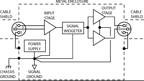
The construction of tie doesn't matter much. What does matter is the location of this bridge. Separate grounds should be tied at the main power supply capacitor, as schematically illustrated below: enter image description here

You need to determine where this point is in your design, but it doesn't look like it is at the corner where you placed the bridge.

\$\endgroup\$
4
  • \$\begingroup\$ So placing the net-tie further away from the main power supply is completely opposite of how to achieve good performance? This is the first time I tried to use separated ground planes in a design. \$\endgroup\$
    – AlexT
    Commented Jun 29, 2018 at 20:18
  • \$\begingroup\$ @AlexT, the main idea is to avoid return ground currents from high-consuming and/or noisy blocks from flowing along grounds from fine and sensitive analog circuits. \$\endgroup\$ Commented Jun 29, 2018 at 20:41
  • \$\begingroup\$ Ali, do you have a sample layout at the net-tie that I can take a look? Thanks! \$\endgroup\$
    – AlexT
    Commented Jul 1, 2018 at 0:48
  • \$\begingroup\$ @AlexT, take a look at various application notes regarding "mixed-signal" designs, like this one, ti.com/lit/an/slyt512/slyt512.pdf Analog Devices should have many analogous notes. \$\endgroup\$ Commented Jul 1, 2018 at 0:56

Your Answer

By clicking “Post Your Answer”, you agree to our terms of service and acknowledge you have read our privacy policy.

Not the answer you're looking for? Browse other questions tagged or ask your own question.