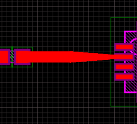
I am designing an RF board in Altium where due to the dielectric selected and its thickness, the trace width for a 50 ohm characteristic impedance is thicker than some of the SMD component pads. What is the best method for routing a larger RF trace to a small SMD pad to minimize the impedance mismatch?
I am currently using the teardrop tool to taper the line down gradually to the smaller width (see below)

