This is a traditional application from CRT deflection circuitry: S-correction.
I have no idea if design resources exist anymore (probably handbook scans can be found somewhere?). See for example this patent:
US 595584 Horizontal deflection S-shaped correction signal circuit with variable capacitance
Or the explanation here: Electronics Now, March 1999, page 8, Service Clinic - Monitor Deflection Circuits.
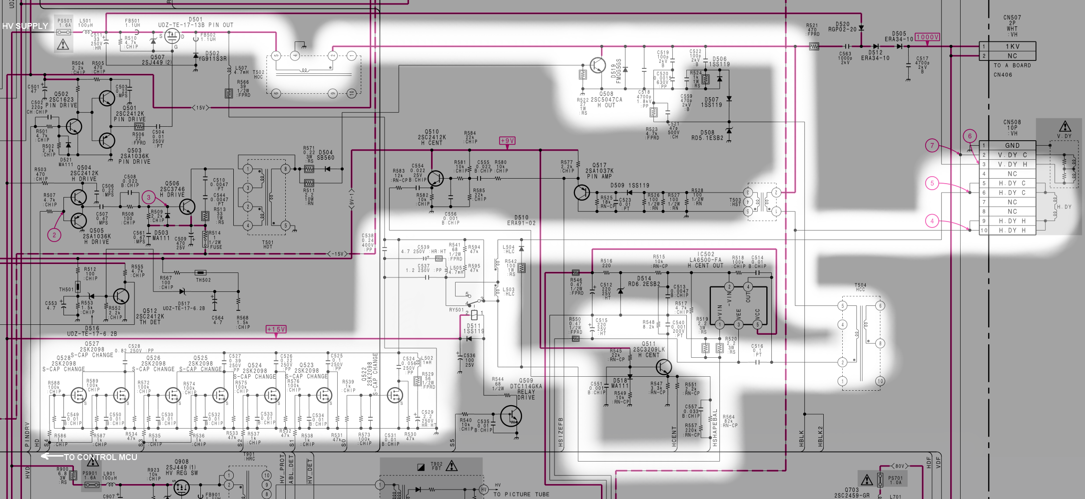
For a practical case, consider this excerpt from a Sony Trinitron monitor, N3 chassis:

Power enters top-left (+200V or so), and passes through the pincushion output Q507; T502 is a choke supplying power to the output transistor Q508; deflection current follows the top and right lines, through T503, to the deflection coil, far right. Deflection current returns through L503 and L504 (center) (depending on the relay state; this gives the clicking sound heard when switching between high and low resolution screen modes), and probably a parallel path through T504 and the H-center circuit (bottom right). The bulk of the current returns to ground through C537 and C538, I think, while a parallel path sinks a harmonic current through a variable capacitance -- S-correction (bottom left).
The remainder of this discussion concerns the bottom-left block.
Note that each individual channel is simply a common-source switch, driven from a logic-level signal (well, gate level, certainly 5 to 15V; the 2SK2098 appears to be logic-level capable so it may well be 5V), with a 47k pull-down resistor on the drain, and the series capacitor to the common node.
When each transistor switches on or off, a big gulp of charge is injected into the deflection circuit. For a monitor, this doesn't matter; it'll take a second or so for the display to settle on switching modes anyway.
Note that bidirectional switches aren't required, as long as the drain self-bias and charge injection at switch-on, is acceptable. Bias is achieved by the internal body diode (note the arrow inside the MOSFET symbol), and the resistor simply prevents the voltage from floating away (excessive voltages could damage the transistor).
The biasing values are all rather inconsequential: 1k series gate resistors (R586, etc.), 100k gate pull-downs (R588, etc.), 47k drain pull-downs (R534, etc.; note that R534 is in parallel with two MOSFETs, whereas R532 for example does only one; yet they're the same values).
Note also the approximate binary sequence of capacitor values: C524-C528 include 56, 100, 220, 390 and 820 nF. Two MOSFETs are used in parallel for the largest values, to help share current. This makes a sort of "power DAC", where for a 5-bit binary code input, 32 unique output values can be selected.
I don't know how many of these lessons can be applied to the present question, but this historical application should at least provide some food for thought.
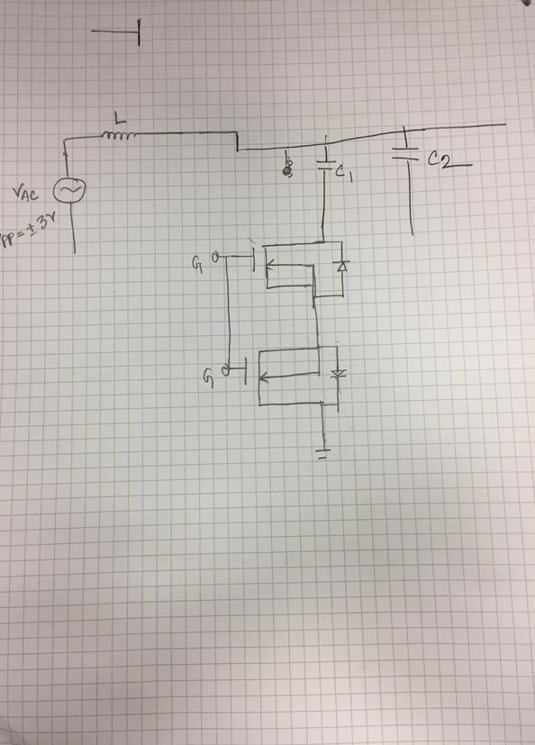
As for the case when a bidirectional switch is required (that is, to more or less answer the question proper): use an isolated gate drive, referenced to the (now floating) pair of source pins. This will pull down to GND when the switch is on, but floats at or below GND when off.


