0
\$\begingroup\$

I have an LVDS clock signal that goes to several PCB cards. Frequency: 100Hz --> 20MHz

I am going to use a fan out IC to supply each card with it's own buffered CLK signal; I am not going do a 'Multidrop Connection'.

  • PCB cards are isolated from each other and the LVDS driver (floating SMUs).
  • Some cards may not be isolated from the LVDS driver.
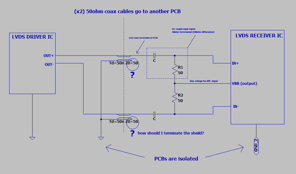
  • The LVDS clock signal is feed into the PCB card(s) using (x2) 50ohm coax cables.
  • The signal is AC terminated to 50ohms and biased by the receiver IC.

How should I terminate the coax shield?

*I do not have and earth/chassis ground in this system. It is a prototype, the PCBs are not enclosed.

There is a PCB card (12v) Supply Voltage reference that powers the on-board isolated DCDC converters on the card(s). However I do not want to use this at the moment because some PCB cards may not be isolated, doing this will cause ground loops. And the grounding scheme of LVDS is still undetermined, I have not designed that part yet.

Basically I want something that will 'work' regardless of how the PCB card(s) and the LVDS driver are referenced, without a chassis ground.

Is there a solution I could do that will be satisfactory? Thanks.

He is the circuit: enter image description here

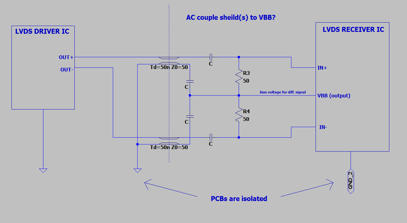
proposed solution 1 enter image description here

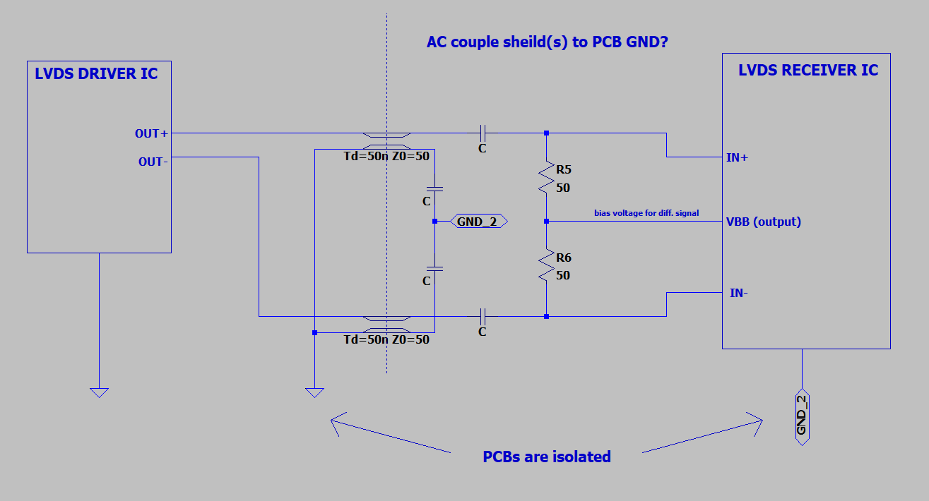
proposed solution 2 enter image description here

\$\endgroup\$
3
  • \$\begingroup\$ Is the use of dual BNC mandatory ? For a differential signal such as LVDS clock, it might be better to use something like twisted pair. I guess this can be brought close enough 100 Ohm impedance to work... If you use two different cables, then the cable loop will pick up magnetic fields and create a lot of jitter. \$\endgroup\$
    – tobalt
    Commented Jun 16, 2021 at 16:49
  • \$\begingroup\$ Which LVDS receiver you are using? What is the common mode range or absolute maximum range for the input? \$\endgroup\$
    – Justme
    Commented Jun 16, 2021 at 17:28
  • \$\begingroup\$ SY100EP195VTG. Its not actually a receiver, but it is where the LVDS CLK signal terminates. I am going to use it to control each cards timing. It says the CMR is 2-5v. I am going to use it as shown in figure 8-3 (pg19). ww1.microchip.com/downloads/en/DeviceDoc/… \$\endgroup\$
    – Tony
    Commented Jun 16, 2021 at 18:33

1 Answer 1

1
\$\begingroup\$

Of your drawn circuits, the last one with caps to GND2 will be best to shunt Common Mode noise. The one with caps to the common mode voltage will be worse, because you want to clamp the shield voltage to a low impedance node (e.g. GND)

However, the use of two physically separate cables for the LVDS lanes is questionable. You form a large loop, into which magnetic fields can couple and become differential mode signals. I anticipate this will create tons of jitter. Probably you are better off with a little impedance mismatch and proper UTP/STP cabling. You can add some resistor in parallel/series to the driver to adapt it to the TP cable.

At the minimum, twist the two BNC cables together tightly.

\$\endgroup\$
1

Your Answer

By clicking “Post Your Answer”, you agree to our terms of service and acknowledge you have read our privacy policy.

Not the answer you're looking for? Browse other questions tagged or ask your own question.