3
\$\begingroup\$

I have the following question regarding gate driving loss in a synchronous Buck. When we want to turn on HS or LS we have to charge their input capacitance \$C_{\text{iss}}\$. This is done through a driver which is supplied by \$V_{\text{dd}}\$ and in it simplest form it can be considered a CMOS inverter. So suppose we are turning on a LS nMOS gate driving loss \$P_{\text{driving}}\$ is defined as

$$P_{\text{driving}}=C_{\text{iss}}V_{\text{dd}}V_{\text{batt}}f_{\text{sw}}$$

A certain charge \$Q_{\text{g}}=C_{\text{iss}}V_{\text{dd}}\$ is provided by the driver and I'm totally fine with it.

Now we are using the pMOS of our CMOS inverter to provide a path between \$V_{\text{dd}}\$ and gate switch. pMOS is operating in triode mode so there will be some heat dissipation or power loss since it behaves like a resistor. At this point I would write average power

$$P_{\text{driver}}=V_{\text{dd}}I_{\text{dd}}$$

where \$I_{\text{dd}}\$ is the current flowing from supply to driver to gate switch. Now if I want to calculate total power loss regarding driving is it right to sum up the two power losses? I've read several application notes but this thing isn't clear: some mention an IC power loss (which should be \$P_{\text{driver}}\$), others never talk about actual power dissipated by the driver. We need power to turn on the LS but we need power also for the driver. And gate driver power consumption impacts overall efficiency.

\$\endgroup\$

2 Answers 2

3
\$\begingroup\$

You are on the right track.

Your total loss is Vdd.Idd . On each turn-on cycle, a charge Qg is consumed from Vdd and delivered to the FET's gate. This (resistive via a FET) charging is precisely 50 % efficient -- half the energy consumed from Vdd is dissipated in the driver, and the other ½ is stored in the gate capacitance.

Note that gate capacitance isn't constant as the FET switches. it is better to characterize the device's switching gate charge which is well defined.

In the subsequent turn-off cycle, all this stored energy is dissipated in the driver's NMOS device.

So -- when charging, an energy E=Qg.Vdd is extracted from Vdd (this happens at a frequency fSW, so the power is Qg.Vdd.fSW). You end up with an energy stored in the gate of ½.C.Vdd^2, or ½.Qg.Vdd (since C = Q/V). The other half of the energy consumed is dissipated in the driver, adding the total Qg.Vdd.

Then, when discharging the FET, all the remaining stored energy (½.Qg.Vdd) is dissipated in the switch.

Therefore, in the end, the total power loss is Qg.Vdd.fSW, or Ciss.Vdd^2.Fsw when the driver is powered by Vdd. If it is powered (e.g. with a linear regulator), the regulator's efficiency changes the Vdd^2 term to Vdd.Vbatt

\$\endgroup\$
3
  • \$\begingroup\$ Thanks very much for the response. In my testbench i have an n-n configuration supplied by Vbatt and two drivers supplied by Vdd. Drivers are made by a chain of inverters. What i was doing is calculate Vdd*Idd and then add QgVddfsw where Q is obtained by integrating current supplied by driver over a period. Basically something similar to this fscdn.rohm.com/en/products/databook/applinote/ic/power/… where driver loss is called IC loss \$\endgroup\$
    – KiDMiO
    Commented Aug 21, 2021 at 19:57
  • \$\begingroup\$ In that document, Icc is not associated with the drivers or FETs, but the remainder of the DCDC's controller -- opamps, bias etc. \$\endgroup\$
    – jp314
    Commented Aug 21, 2021 at 20:20
  • \$\begingroup\$ Ok thanks very much so by calculating QgVddfsw i obtain the total driving losses which should be equal to Vdd*Idd and comprehend everything from driver to driving process \$\endgroup\$
    – KiDMiO
    Commented Aug 21, 2021 at 20:30
2
\$\begingroup\$

You should not attempt to calculate these kinds of losses using capacitance related to your MOSFET switch as this will yield inaccurate results.

The capacitances are time-varying and in very non-linear ways, so you have to use the integral of current with respect to time (charge) instead.

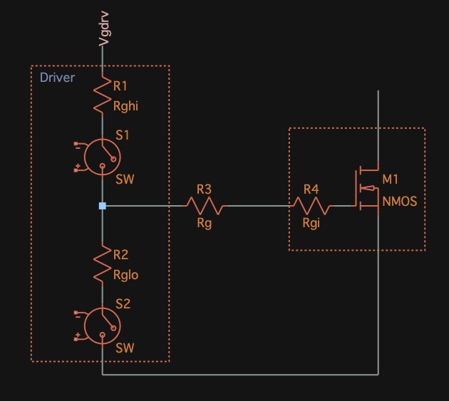
The power loss in your driver is best calculated by modeling your driver's high and low MOSFETs as resistances (especially if your high side driver FET is in the triode region) like so:

$$ P_{driver} = \frac{V_{gdrv}Q_{Gtot}f_{sw}}{2} x \left ( \frac{R_{GHI}}{R_{GHI}+R_{G}+R_{GI}} + \frac{R_{GLO}}{R_{GLO}+R_{G}+R_{GI}}\right )$$

Where:

  • \$ V_{gdrv}= \$ Gate driver voltage (the power supply voltage)
  • \$ Q_{Gtot}= \$ Total gate charge of the LS MOSFET
  • \$ f_{sw}= \$ Switching frequency
  • \$ R_{GHI}= \$ High side driver resistance
  • \$ R_{GLO}= \$ Low side driver resistance
  • \$ R_{GI}= \$ LS MOSFET gate resistance
  • \$ R_{G}= \$ Series gate resistance

Or like this:

enter image description here

As you can see, you can very directly impact and reduce the driver power dissipation by increasing \$ R_{G} \$, but at the cost of increasing turn on and turn off times in the LS MOSFET. Depending on your specific specs and chosen MOSFET, adding or increasing the value of a gate resistor can actually result in higher total efficiency for the whole device. Or make it worse. It is definitely something you need to consider however when looking at the whole circuit efficiency.

\$\endgroup\$
1
  • \$\begingroup\$ Ok thanks so if i have the current flowing into the driver i multiply it by Vgdriv (instantaneous power) and then by integrating it i find gate charge loss right? do i have also to add power across Rglo? \$\endgroup\$
    – KiDMiO
    Commented Aug 27, 2021 at 11:19

Your Answer

By clicking “Post Your Answer”, you agree to our terms of service and acknowledge you have read our privacy policy.

Not the answer you're looking for? Browse other questions tagged or ask your own question.