-1
\$\begingroup\$

I need to supply logic 1 or 0 (selected by a DIP switch) to NAND gates. Input 'A' & 'B' are inverted to each other. My Question: 1: Is the below circuit okay or its better to use inverter IC on A to supply B?

2: Is there any difference in using pull-up vs pull-down resistor in this case?

3: what can the max R1 value be? I want to have minimal current draw (when the switch is ON for logic '1') through the pull down resistor.So I should use the highest resistor value ?I know R1 is determined by the type of NAND chip (CMOS /TTL), so next question which chip should I use? My application will have regulated 5V supply and won't be >1KHz operating freq.Just need low power consumption. Is the selected 74HC132 okay?

Sorry for the basic question but I am just trying to understand the basics to actually implement my design from proteus simulator to PCB. enter image description here
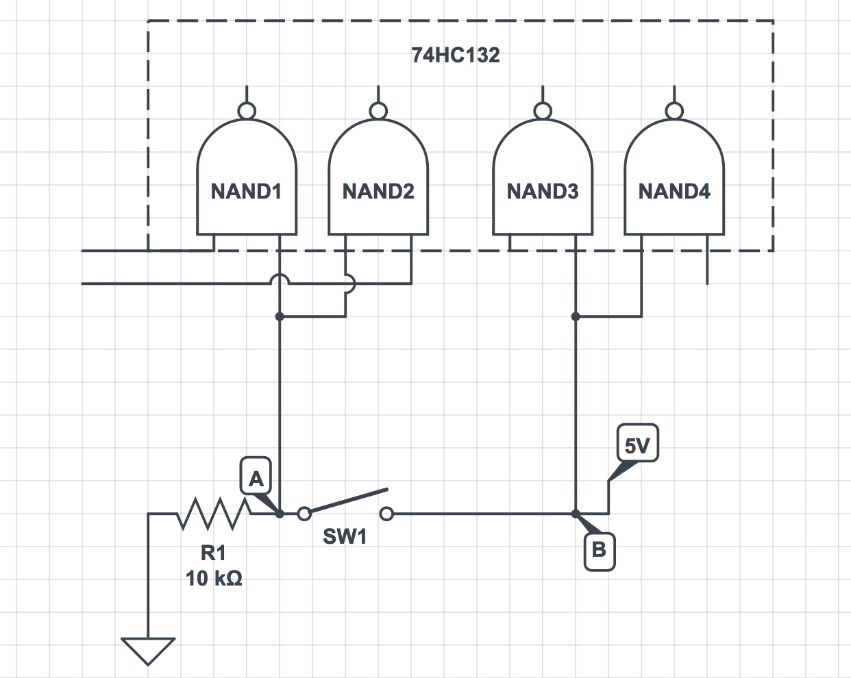
EDIT: just found out that Input 'B' will always have 5 V. So I will need another DIP swicth-pulldown resistor combo OR invert 'A' to supply 'B'.

\$\endgroup\$
4
  • \$\begingroup\$ B is always high in your diagram ... the switch has no effect on its voltage level \$\endgroup\$
    – jsotola
    Commented Jun 18, 2022 at 3:56
  • \$\begingroup\$ Yes, now that you mention it. It is always 1. Oops. I can just supply 'B' through either using second DIP switch and separate pulldown resistor. OR maybe use an invertor on 'A' to generate 'B' . \$\endgroup\$
    – eaterbugs
    Commented Jun 18, 2022 at 4:37
  • \$\begingroup\$ "I want to have minimal current draw (when the switch is ON for logic '1') through the pull down resistor." - define 'minimal'. \$\endgroup\$ Commented Jun 18, 2022 at 6:36
  • \$\begingroup\$ I don't have a specific value in mind. But my reasoning is why have .5mA draw if we can get just 5uA being drawn(with 1MOhms). I am looking for the biggest resistor value that I can use here which has the smallest current draw without radically redesigning the circuit. Unless I am missing something. \$\endgroup\$
    – eaterbugs
    Commented Jun 18, 2022 at 7:54

1 Answer 1

1
\$\begingroup\$

As already in the comments, the circuit as is has an issue with B always being high.

A 2nd switch will add another pull up/down resistor and minimum current being the objective. But an extra inverter adds small load current as well. Other 2 switch considerations, could something bad occur if B is not the inverse of A? This would make 2 switches undesirable as they could be set to violate this need. Obviously an inverter is cleaner.

The maximum resistance will be a function of the input leakage current expected and VIH VIL (or for the Schmidt device mentioned VT+ VT-). Basically the resistor must be capable of actually pulling the voltage to the permitted range. Maximum input leakage current is 1uA per pin (+85C) but x4 s there are 4 pins used so 4uA. Worst case tolerable voltage drop based on VT- = 0.9 (Vcc=4.5V). So Rmax = 0.9/4uA = 225kOhms. BUT this does not account for wiring/switch leakage and that is harder to estimate, so the value used should be lower.

(A bit of irony; the PC I'm typing this on has its power switch disconnected from the motherboard as it is a very leaky 60kOhms and would randomly turn the PC on and off. Clean dry environment but many years of use)

As to pull up or down, assuming the input will spend equal time set high and low, it makes little difference. But if the switches are more commonly in one state then the switch should be configured such that it is open in this state. In the above circuit if A is mostly going to be set low then R1 is wired optimally.

\$\endgroup\$

Not the answer you're looking for? Browse other questions tagged or ask your own question.