0
\$\begingroup\$

Background:

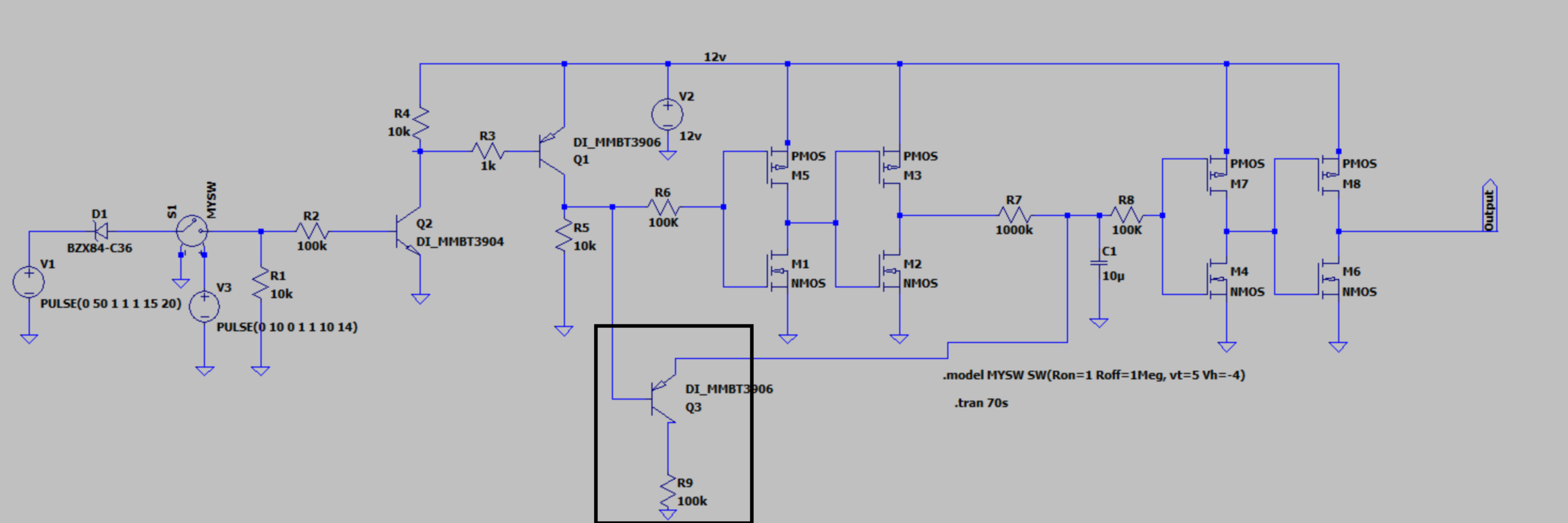
I have the following circuit. The circuit leading up to the mosfets(buffer structure) basically turns the output high if both a specific voltage (>~37) and switch MYSW is pressed. Two buffer stages are included(this will be replaced with a buffer IC). They are there so that an RC delay can be introduced after the conditions are met and to not load the next stage.

One issue i had was that this would also introduce a turn off delay as C1 would discharge through R7. To fix this a new discharge path is included which activates as soon as the conditions for the circuit are not met anymore.

Actual question:

The first circuit with the black box highlighted uses a PNP to quickly discharge the output cap. The resistor at the bottom doesn't appear to make much of difference to the discharge time (why?). The cap discharges quite rapidly as the base drops. The intention is to use it as a switch, so that when the base drops, C1 discharges rapidly R9.

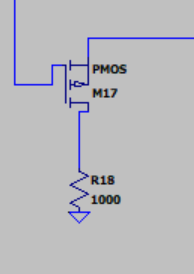
Also how does this circuit compare with had a mosfet been used instead as shown in the second picture. Changing R18 now is changing my discharge time (although it is slower than the discharge of the BJT).

Is this a result of not ensuring the mosfet stays in triode region and/or the bjt not staying in the saturation region and so the circuit is not behaving as a switch as i intend it to be? How would i resolve this and the better way of doing so?

enter image description here

enter image description here

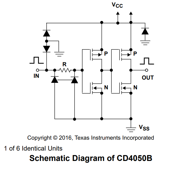
Example of buffer IC internal structure: enter image description here

\$\endgroup\$
5
  • \$\begingroup\$ First, Q1 is upside-down. You're forcing it into "reverse active" mode. Second, why not just split the connection between M2 and M3, leaving R7 connected to M3. Then, connect R9 between C1 and M2 and forget about Q3 altogether. \$\endgroup\$
    – Dave Tweed
    Commented Nov 18, 2022 at 12:14
  • \$\begingroup\$ @DaveTweed thanks for pointing that out. I forgot to mirror it when i copied the circuit for this question. I have fixed the said error on the schematic \$\endgroup\$
    – Hasman404
    Commented Nov 18, 2022 at 12:25
  • \$\begingroup\$ Whilst the suggestion is good, i am intending on using a buffer IC which has its output push pull tied (as shown in the additional image) and so can't make the circuit like that. \$\endgroup\$
    – Hasman404
    Commented Nov 18, 2022 at 12:26
  • \$\begingroup\$ Whatever. In any case, the Q3/R9 combination doesn't work well because there's a second discharge path through the BE junction of Q3 and R5. The M17/R18 solution avoids this problem, but it operates M17 in "source follower" mode, in which it can't discharge the capacitor below its own threshold voltage. It would be better to use an NMOS with its source tied to ground, and an inverted drive signal for the gate. \$\endgroup\$
    – Dave Tweed
    Commented Nov 18, 2022 at 12:35
  • \$\begingroup\$ You could remove R9 entirely and Q3 would still discharge the cap, because in your current circuit the primary discharge path is through Q3's b-e junction and R5. \$\endgroup\$
    – brhans
    Commented Nov 18, 2022 at 15:46

1 Answer 1

1
\$\begingroup\$

Do away with Q3 and place a diode across R7 (anode towards C1).

This will rapidly discharge C1 via the diode when the output of the first buffer goes low.

It would probably be a good idea to place a low value resistor between the R7/diode combination and the output of the first buffer to limit the peak discharge current to protect the buffer.

\$\endgroup\$
1
  • \$\begingroup\$ You can also put R9 in series with the diode. \$\endgroup\$
    – Dave Tweed
    Commented Nov 18, 2022 at 13:42

Your Answer

By clicking “Post Your Answer”, you agree to our terms of service and acknowledge you have read our privacy policy.

Not the answer you're looking for? Browse other questions tagged or ask your own question.