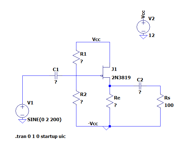
The component values of this circuit are extremely non-critical. R1 and R2 especially can be off by an order of magnitude from their ideal values without affecting the circuit much.
Let's start with Re, since this part is the only one that has to be somewhat accurate. To make it simple, let's operate the JFET at its minimum guaranteed Idss (zero gate-voltage drain current). The datasheet specifies it as 2mA. This means that any 2N3819 will always be able to pass at least 2mA with a gate-to-source voltage of 0V or less. This gives us the lowest possible output impedance within the datasheet's guaranteed characteristics for this JFET.
Let's also assume that you want to bias the output voltage (J1 source pin) at 4V. This is a rather arbitrary choice, but it leaves some headroom in case the JFET is better than specified and needs some negative gate-source voltage to turn it off enough so that it only passes about 2mA. (If the JFET is better than the datasheet minimums, the output quiescent voltage will go up, and we don't want it to bump into the supply voltage.)
As a result, we want Re to drop 4V when 2mA pass through it. This means Re = 200 Ohms.
Next, you'll have to choose R1 and R2. Since we chose to operate the JFET at Idss, its gate voltage equals the source voltage (at least if we get a 2N3819 that actually has Idss=2mA; it can and will vary). This means that the gate voltage must be 4V, so R1 and R2 have to form a voltage divider that divides the 12V supply down to 4V. Only the ratio of R1 and R2 is critical, not their exact values. Since the gate leakage of the 2N3819 is so low (2nA), you could use R2 = 1 MOhm and then calculate R1 accordingly to get the voltage divider ratio correct.
Last but not least, you'll have to calculate C1 and C2. C1 forms a high-pass together with the Thevenin equivalent resistance of R1 and R2, so it'll have to be big enough to pass the lowest desired signal frequency without much attenuation. C2 forms a high-pass with Rs, the same applies there.
Also, your schematic drawing has some errors (R1/R2 are not actually connected to the JFET gate, and the JFET symbol is wrong, as Andy aka mentioned)

