1
\$\begingroup\$

I am trying to make a WiFi switch using the ESP32 MCU.

The PCB I am building will be switching high-power applicances, such as a kettle (which can draw around 14 A @ 230 VAC). The relay I chose is the ALFG1PF12.

According to the trace width calculator I get the following dimensions for the trace width of 11.44 mm (external):

enter image description here

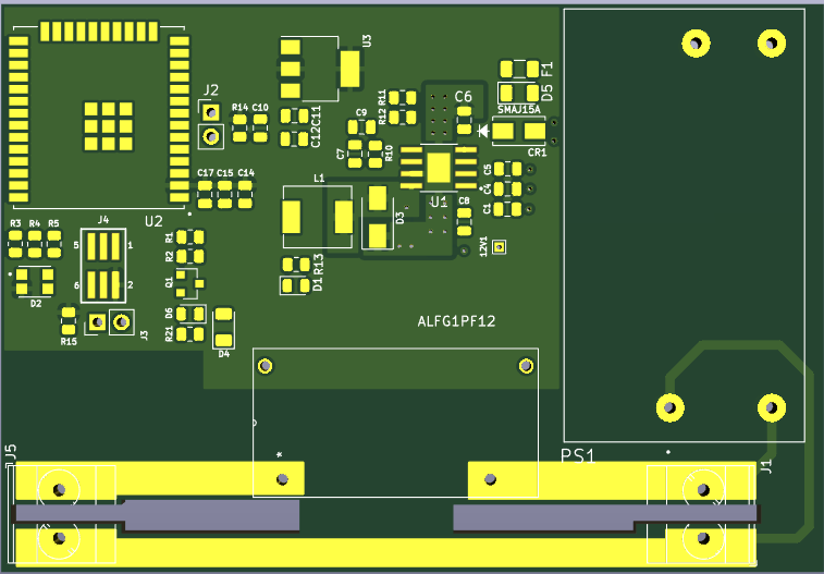
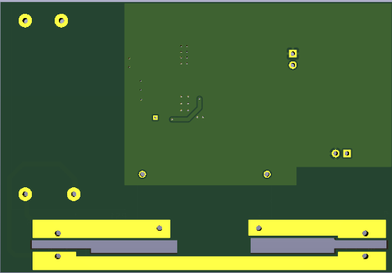
Using an 11 mm trace is quite huge. I saw that some people use the technique of using a bottom trace and top trace and then removing the solder mask. See the below pictures:

enter image description here

enter image description here

My questions:

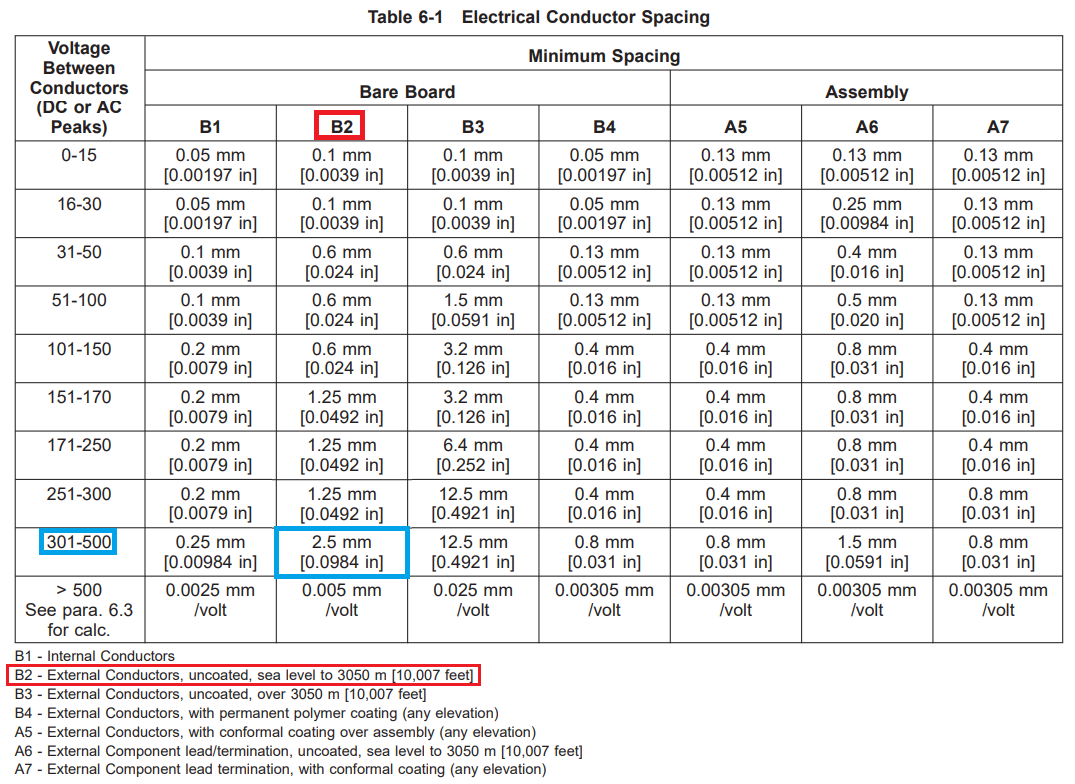
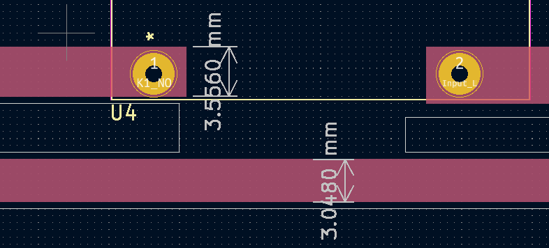
  1. According to the IPC-221A I should require a track spacing of 2.5 mm (column B2). I have a spacing of 3.048bmm. This is above the regulations. Is this statement correct?

enter image description here

enter image description here

  1. I used copper pours (top and bottom) that have a width of 3 mm. Does this mean the effective width is 6 mm?

enter image description here

I also removed the soldermask to add more solder so this will increase the effective width even more. How much of solder do I need to add so the trace can handle the 14 A?

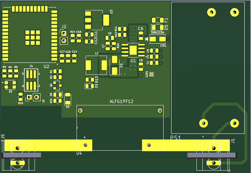
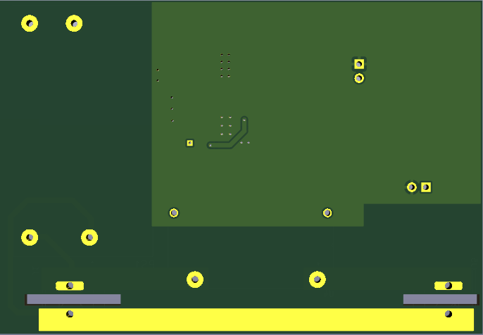
Edit 2:

Top layer enter image description here

Bottom layer enter image description here

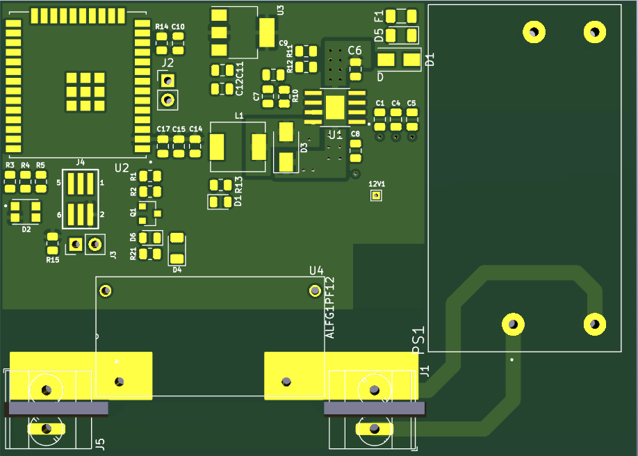
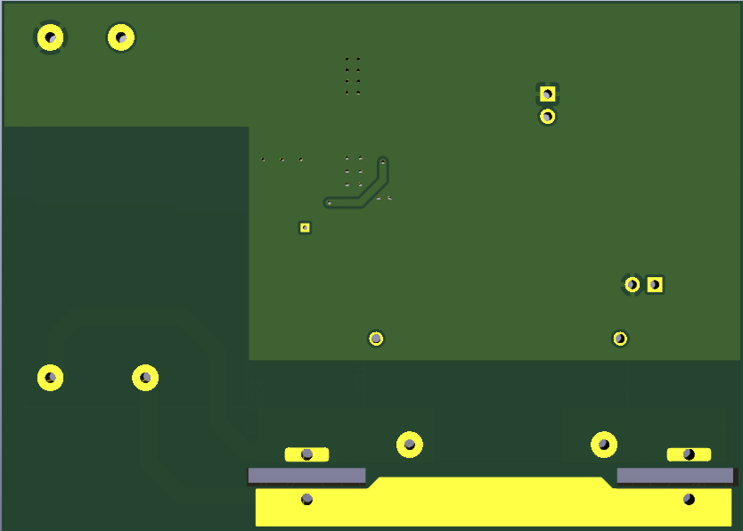
Edit 3:

Top layer enter image description here

Bottom layer enter image description here

\$\endgroup\$
13
  • \$\begingroup\$ How many layer do you use? Should it be compliant world wide? Europe? USA? Are the grey boxes actully slits? \$\endgroup\$
    – datenheim
    Commented Jan 8, 2023 at 19:37
  • \$\begingroup\$ @datenheim this is a two-layer PCB. I am using it in South Africa only. Yes the grey boxes are slits to improve the creepage distance \$\endgroup\$
    – JoeyB
    Commented Jan 8, 2023 at 19:41
  • \$\begingroup\$ Creepage distance has not been improved because the minimum distance over surface is still between the pins of the terminal blocks. \$\endgroup\$ Commented Jan 8, 2023 at 19:44
  • \$\begingroup\$ @TimWilliams thanks for that I forgot to extend the slits into the connectors. Will update the pics. \$\endgroup\$
    – JoeyB
    Commented Jan 8, 2023 at 19:55
  • 1
    \$\begingroup\$ The exposed copper is not so much meant to be reinforced with solder (which has rather bad conductivity), but e.g. with thick copper wire(s) or bars that are soldered onto the trace \$\endgroup\$
    – tobalt
    Commented Jan 8, 2023 at 20:11

1 Answer 1

2
\$\begingroup\$

Creepage

Consider two independent conductors on top and bottom. This is the side view near a board edge or slot: Creepage path between layers The red line is the creepage length.
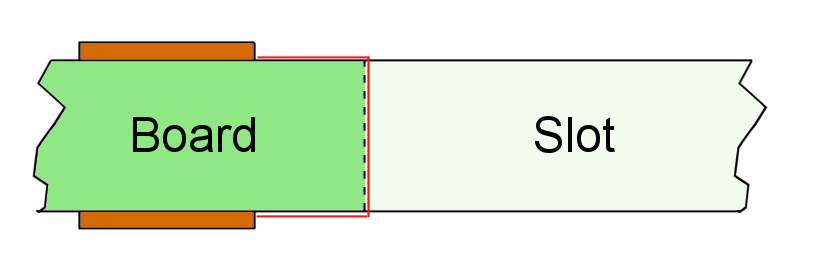
For two conductors on the same layer, slots are needed anywhere they would be too close otherwise (top view):
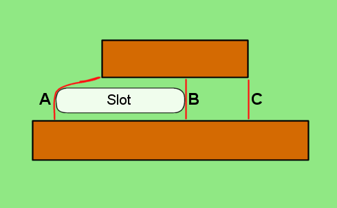
Creepage path over a layer

B and C are equal. The slot has no effect on creepage near it, only paths that would otherwise go through it. Because B and C are less than A, they set the creepage distance. The slot must be extended so that the shortest path is A-like on both ends.

Trace Width

IPC-2152 suggests around 350 mils (8.9 mm) for 14A at 20°C temp rise in 2 oz. (70 µm) copper. If you don't have this space to spare, bulking it up is a good idea.

If this is just a one-off, embedding wire or solder wick (as commented) is a fine solution.

Other options:

  • Expand the PCB outline to fit enough copper width and clearance (can bring back two-sided conductors).
  • Move the connectors to minimize trace length. Note that ampacity calculations assume infinite length traces. Shorter than a couple inches, heatsinking from the connections themselves is significant. For pads closer together than the trace width, width itself becomes meaningless, and ampacity becomes very high.
  • For production, the cost premium of heavier copper or four layers may be justified by the compact outline, if that's the greater value. (Inner layers experience zero creepage and the clearance is much shorter, due to it being through a dielectric instead of air. A major downside is inner layers dissipate heat more poorly, so more width is needed.)
  • Potting could also be used, but this is probably a specialty solution -- when the absolute smallest build is necessary, or very high voltages.

Other

Note that rout slots cannot have square inside corners. If you put them in the design, the fab will most likely choose the largest common end mill that fits, usually 1 mm radius. This won't affect the slots shown, but is something to keep in mind in general. To ensure you get what you are expecting, add inside corner radii to the shapes. Keep the radius on the large side; very sharp corners require very small cutters which work slower and break more easily -- added cost.

\$\endgroup\$
11
  • \$\begingroup\$ I see what you meant earlier on when you said to add the two tracks on opposite layers. Please see Edit 2 above. Do you know how I can beef up those tracks to handle 14A? \$\endgroup\$
    – JoeyB
    Commented Jan 9, 2023 at 11:17
  • \$\begingroup\$ Looks like solder wick seems to be the best option! \$\endgroup\$
    – JoeyB
    Commented Jan 9, 2023 at 11:25
  • 1
    \$\begingroup\$ @JoeyB Yeah, that'll do. More detail added above. \$\endgroup\$ Commented Jan 9, 2023 at 11:44
  • \$\begingroup\$ Thanks, I managed to arrange the components to minimize the track length. See Edit 3 \$\endgroup\$
    – JoeyB
    Commented Jan 9, 2023 at 12:21
  • 1
    \$\begingroup\$ As in, what does it do? Due to surface contamination and other effects, sparks can travel farther along surfaces than through air. Also, soldermask doesn't help much; its thickness is quite variable and it often has pinholes. \$\endgroup\$ Commented Jan 9, 2023 at 13:21

Your Answer

By clicking “Post Your Answer”, you agree to our terms of service and acknowledge you have read our privacy policy.

Not the answer you're looking for? Browse other questions tagged or ask your own question.