0
\$\begingroup\$

I am trying to use the built in ADC of a PIC 18F4520.

The input is a voltage signal from an analog sensor whose output varies with temperature. It comes to be about 5.2 V at a certain temperature.

I am getting fluctuating values from the ADC output (I checked the ADC output by printing the result with 4 seven segment display unit.) When the output seems to be 65 it fluctuates between 60-70. I am unable to understand the cause of this fluctuation.

As I intend to measure temperature via the output of this analog sensor, the fluctuating ADC output is causing trouble.

What can be the reason and a solution?

Is there a way to know the output that 10 bit ADC will show for a particular input?

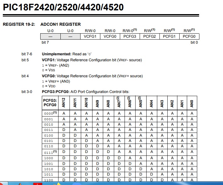
The image gives the ADCON 1 register details.

Image source: Microchip - PIC18F2420/2520/4420/4520 Data Sheet

I am also confused that if I had set the reference voltage bit VCFG0 to VDD i.e. 5 V. and VCFG1 to VSS i.e. 0, will my ADC be able to measure 5.2 or any voltage above 5 V?

\$\endgroup\$
6
  • \$\begingroup\$ newbie - Hi, Please remember the site rule which requires that when a post includes content (e.g. text, image, photo etc.) copied or adapted from elsewhere, that copied content must be correctly referenced. As a minimum, the source webpage or PDF etc. should be linked (see that rule regarding references for books / articles etc.). In order to help you, I found what I believe to be the source PDF link & added it for you. For the future, please remember it's your responsibility to do that :) Thanks. \$\endgroup\$
    – SamGibson
    Commented Jun 22, 2023 at 17:54
  • 1
    \$\begingroup\$ newbie - Hi, Can you please edit your question to add your schematic, including its power sources. Also link to the sensor's datasheet and any relevant extra schematic (not already on the MCU schematic) showing any conditioning of that signal. The 5.2 V analog input is a concern. What do you mean by "the output is 60 it fluctuates between 60-70" - something can't be a (fixed) 60 and also fluctuating between 60-70 so somehow you must be referring to different things / measurements, but I don't know what they are. I'm guessing one is that 4x7-segment "display unit". Is that a voltmeter? \$\endgroup\$
    – SamGibson
    Commented Jun 22, 2023 at 18:00
  • \$\begingroup\$ Can you tell how to calculate the adc output for a given voltage. Assuming 10 bit ADC and Vref+ = 5V and Vref_ =0V . \$\endgroup\$
    – newbie
    Commented Jun 22, 2023 at 18:13
  • 3
    \$\begingroup\$ newbie - Hi, Your comment a few minutes ago seems to be asking the same as part of the original question i.e. to calculate the ADC output for a given voltage. I don't know why you wrote that as a comment, as it's already in the question. If you are trying to make the question clearer by adding that comment, then don't do it that way - instead edit the question if you're trying to improve/clarify it. || I see you've edited the question slightly ("is 60" to "seems to be 65") but that doesn't answer any of the points where I requested clarification. Hopefully someone else can help. \$\endgroup\$
    – SamGibson
    Commented Jun 22, 2023 at 18:23
  • 1
    \$\begingroup\$ The ADC should not be able to measure anything above Vref. Consider a resistor divider from the voltage signal, where the highest/lowest temperatures produce 4.9V/0.1V (the most usable resolution.) May have to use an opamp to both scale and ensure that the output never goes above Vdd or below Vss. \$\endgroup\$
    – rdtsc
    Commented Jun 22, 2023 at 19:39

1 Answer 1

0
\$\begingroup\$

This is from page 225 of the datasheet:

enter image description here

Left justified means that the ADC result is stored in the upper 10 bits of the 16 bit conversion result, with bits 0 to 5 being (presumably, I couldn't find more information about this) zero. Right justified means that the 10 bit result is in bits 0 to 9, and bits 10 to 15 are zero.

This means that depending on the justification you have selected, the conversion result could range from:

\$0\cdots 1111111111000000_2 = 0\cdots 65472\$ (left justified), or

\$0\cdots 0000001111111111_2 = 0\cdots 1023\$ (right justified)

An ADC input \$V_{IN}\$ will produce a conversion result \$N\$ as follows:

\$ N = (V_{IN}-V_{REF-})\frac{65473}{V_{REF+}-V_{REF-}} \$ (left justified), or

\$ N = (V_{IN}-V_{REF-})\frac{1024}{V_{REF+}-V_{REF-}} \$ (right justified)

If you software configure the ADC to use the supplies \$V_{DD}\$ and \$V_{SS}\$ as references, you have \$V_{REF+}=+5V\$ and \$V_{REF-}=0V\$, which corresponds to:

\$ N = V_{IN}\times 13094.6 \$ (left justified), or

\$ N = V_{IN}\times 204.8 \$ (right justified)

The significance of the ±5 count deviation you mentioned (60 to 70) would suggest that you are using right justification, since a change in the least significant bit of a left-justified result (bit 6) would cause the conversion result to change by \$2^6=64\$.

±5 counts out of 1024 is an error of ±0.5%, which is quite bad. Under ideal conditions, this ADC can perform better than ±0.2%. I would hazard a guess at three possible sources of error:

  1. The sensor is powered from a noisy supply, and its output contains some element of supply noise. Without more information about the senor, I can't comment further.

  2. The voltage reference for the ADC is derived from a noisy supply, and will contain noise for the same reason. This can be mitigated by using an external voltage reference, such as the TL431.

  3. There is a layout or signal path impedance problem, causing the ADC input to have noise induced within it from nearby sources of interference. This is a huge topic, too big to cover here. Solve 1 and 2 first, then we can talk about 3.

Lastly, you must never expose any input to voltages lower than \$V_{SS}-0.3V=-0.3V\$, or greater than \$V_{DD}+0.3V=+5.3V\$, and this includes the ADC input. This is described in the "absolute maximum ratings" on page 323. This does not mean that these levels correspond to the conversion range of the ADC; that range is still \$V_{REF-}\$ to \$V_{REF+}\$. To be safe, if your sensor is capable of producing a signal outside of the range 0V to +5V, then you must take measures to protect the ADC input from that.

\$\endgroup\$
2
  • \$\begingroup\$ Thanks for your informative answer. \$\endgroup\$
    – newbie
    Commented Jun 23, 2023 at 8:55
  • \$\begingroup\$ I will check for noise in input signals and will get back. \$\endgroup\$
    – newbie
    Commented Jun 23, 2023 at 9:00

Your Answer

By clicking “Post Your Answer”, you agree to our terms of service and acknowledge you have read our privacy policy.

Not the answer you're looking for? Browse other questions tagged or ask your own question.