4
\$\begingroup\$

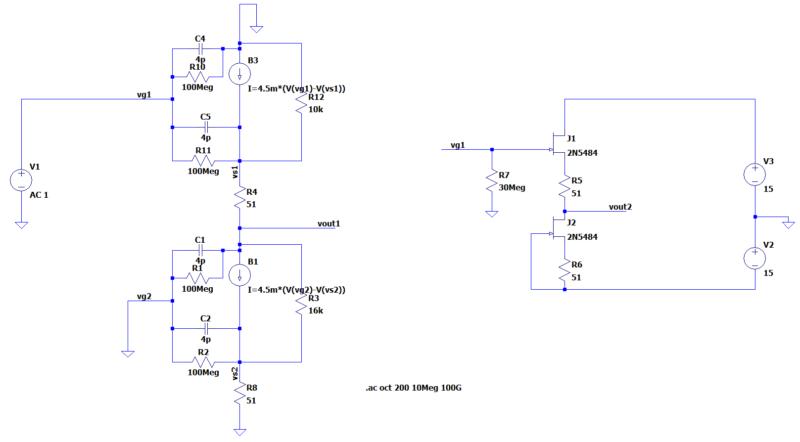
I was solving for poles and zeros of this JFET amplifier with an active load, and found an unexpected zero far off in the response when using the SPICE model. The large-signal and small-signal models are shown below.

enter image description here

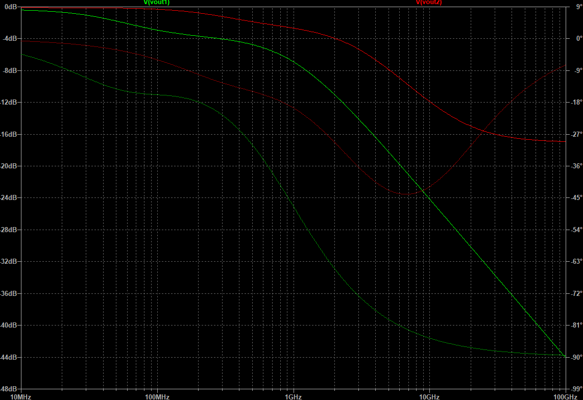
The device parameters (Cgs, Cgd, gm) are more or less approximate, but still, the simulated transfer functions are very different around the break frequencies (green=small-signal model, red=SPICE JFET):

enter image description here

According to the SPICE 3 User's Manual (among other references), level 1 JFET models use the Shichman-Hodges model for FETs, and this model only includes two capacitances, though a third capacitance (Cds) can be included. I've never seen a JFET small-signal model that had other capacitances (probably because in practice for high frequencies the lumped element thing breaks down anyway and we use $y$-parameters).

The thing is, the transfer function for the SPICE version has a zero around 21 GHz, whereas the small-signal model falls off after the (more or less) dominant pole around 1.125 GHz.

The disagreement between these two models is significant, even in the 10MHz - 500MHz region, although adjusting the JFET models can help somewhat by pushing the cutoff around.

But why is there such strong disagreement beyond 1 GHz for these two models? What model does SPICE (or only LTSpice) use that results in the extra zero in the response?

\$\endgroup\$
3
  • 1
    \$\begingroup\$ Does anything change if you use G-sources instead of your B-sources? Generally, you want to avoid B-sources when doing linear analysis. \$\endgroup\$
    – Ste Kulov
    Commented Nov 7, 2023 at 22:14
  • 1
    \$\begingroup\$ No change, and pen-and-paper analysis gave similar results to simulation, with some pole-zero cancellation (approximately), and one pole at around 1.1 GHz. Maybe I can revisit my assumptions and find where the extra zero pops in \$\endgroup\$ Commented Nov 8, 2023 at 1:57
  • 1
    \$\begingroup\$ How are you calculating the capacitances? Change the simulation to .op, then run it and close the report window. Then open the SPICE Error Log (CTRL+L) to see what LTspice internally calculates for the small signal parameters for J1 & J2. Then compare those to your calculations. \$\endgroup\$
    – Ste Kulov
    Commented Nov 8, 2023 at 6:11

1 Answer 1

6
\$\begingroup\$

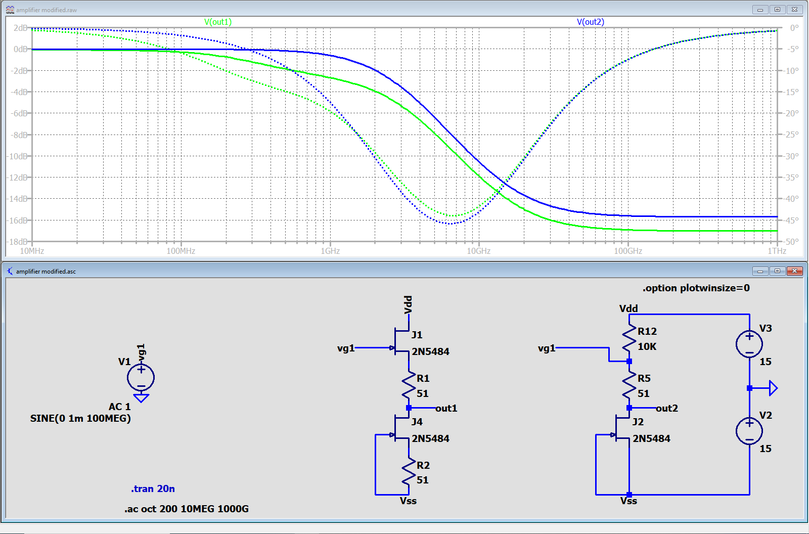
I believe I have an acceptable hypothesis about an origin of this pesky zero in your SPICE simulation. First, notice that this zero is due to an active load of your JFET amplifier. To verify this claim of mine, remove the common-drain-connected transistor J1 from the circuit, replacing it with its output resistance 10K (R12 of your small-signal model). Feed the input signal directly to the node where 10K and 51 Ohm are connected (where there was the J1 source terminal). The simulated transfer function of this new circuit is asymptotically identical to that of the original circuit. The discrepancy of graphs in midrange is understandable and can be easily explained.

amplifier modified

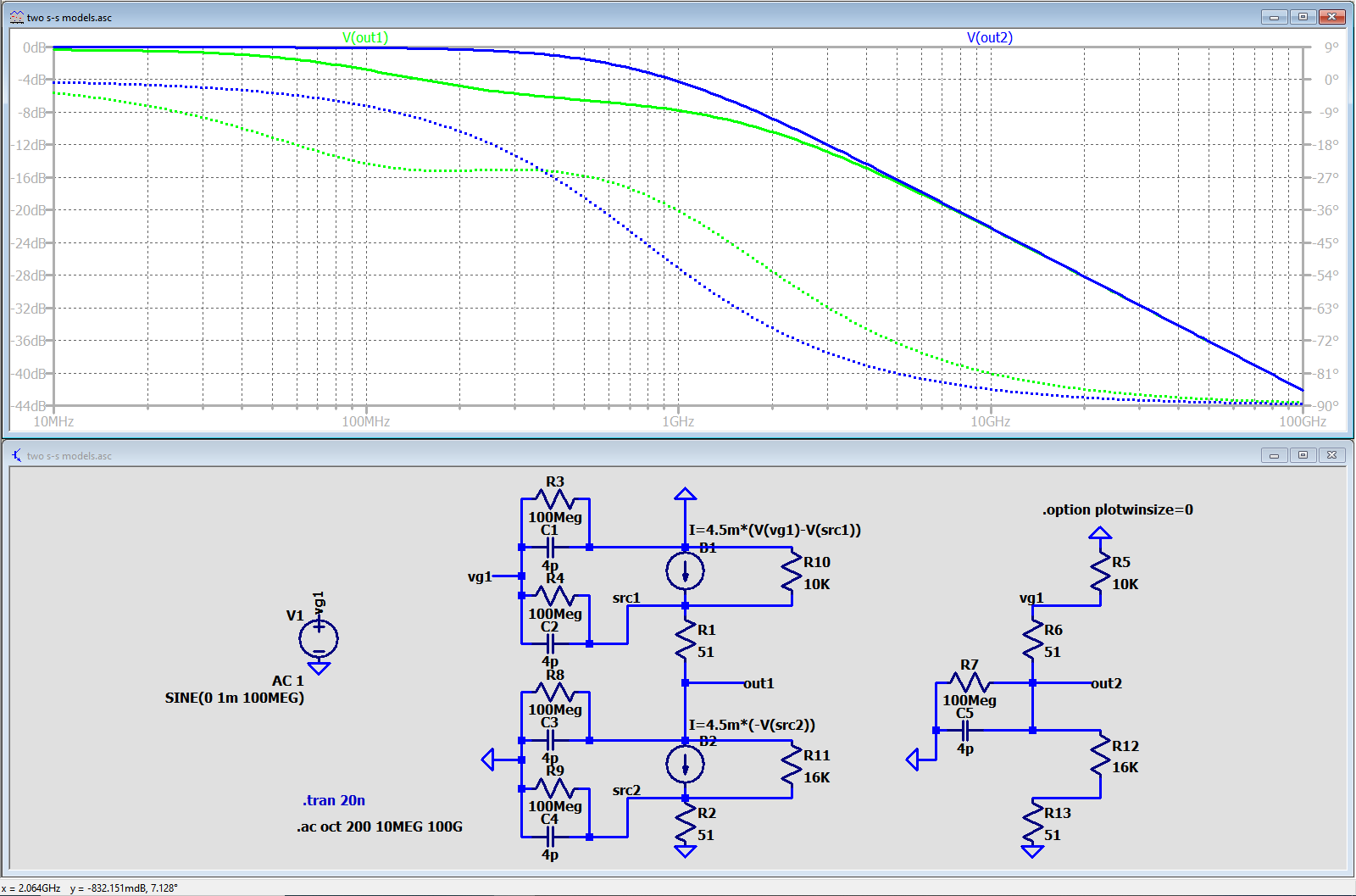
The small signal model should be modified as well: we can remove all the components used to model J1 except for R12 and connect vg1 directly to the vs1 node. As V(vg2)=0 (gnd), the behavioral current source I=4.5m*(V(vg2)-V(vs2)) (B1 in your circuit) does not contribute into the transfer function of the small signal model. Likewise, you can get rid of R3(16K), R2(100MEG), C2(4p) and R8(51). The modified small model demonstrates the simulated transfer function which is asymtotically identical to that of the original small signal model, if we modify C3 (Cgd) value to 1p. The discrepancy of graphs in midrange is understandable and can be easily explained.

ss models comparison

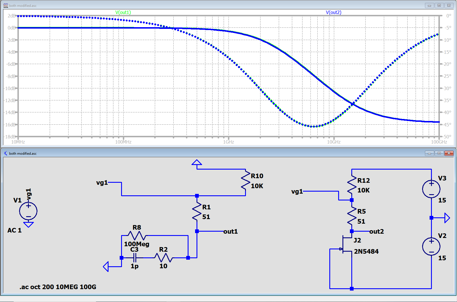
And now, my conjecture. The gate and drain terminals have a resistance (besides, of course, inevitable leakage) that is connected in series with the gate drain capacitance Cgd. Setting the value of this series resistance to 10 Ohm and modifying the value of Cgd to 1p, we run the simulation:

bingo

The simulated transfer functions are identical for both the modified transistor model and the modified small-signal model. You clearly see that introducing the resistance of JFET terminals in series with the gain-drain capacitance produces a coveted zero of the transfer function, and that quite reasonable parameter values can be used to reach an agreement not only on qualitative, but also on quantitative terms.

\$\endgroup\$
3
  • 3
    \$\begingroup\$ Ah, RS and RD must be applied outside of the capacitance; neat. \$\endgroup\$ Commented Nov 8, 2023 at 11:11
  • 3
    \$\begingroup\$ Love it, excellent work. Big bonus points for showing your process of tracking this down, I definitely learned something here. \$\endgroup\$ Commented Nov 8, 2023 at 11:25
  • 1
    \$\begingroup\$ It is a good question, articulated well. I did my utmost to answer. \$\endgroup\$
    – V.V.T
    Commented Nov 8, 2023 at 13:25

Your Answer

By clicking “Post Your Answer”, you agree to our terms of service and acknowledge you have read our privacy policy.

Not the answer you're looking for? Browse other questions tagged or ask your own question.