0
\$\begingroup\$

I would like to know why the IPC 2221 standard requires spacing much larger than necessary from a dielectric strength consideration.

My first question is related to the distance d_1 of the sketch below (distance between copper traces in same layers covered by solder stop).

PCB sketch

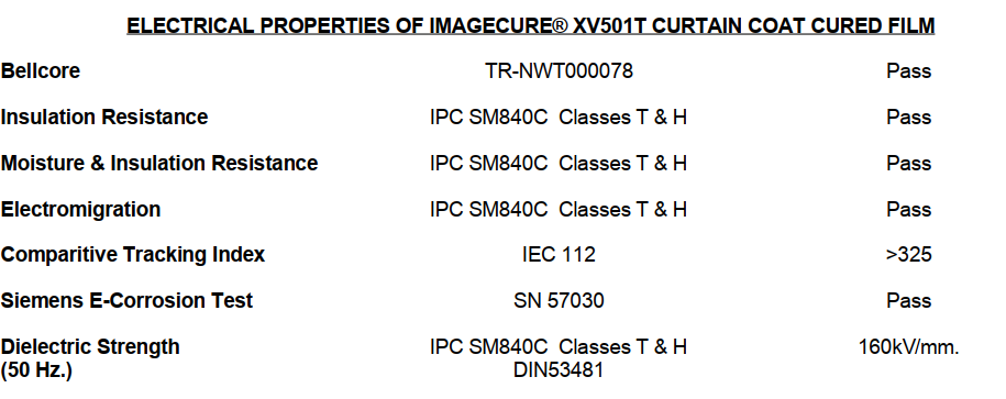
The datasheet of the Coates Imagecure XV501T solder stop material gives a dielectric strength of 160 kV/mm:

enter image description here

Therefore, a maximum voltage of 16 kV could be sustained between two traces 0.1 mm apart, am I right?

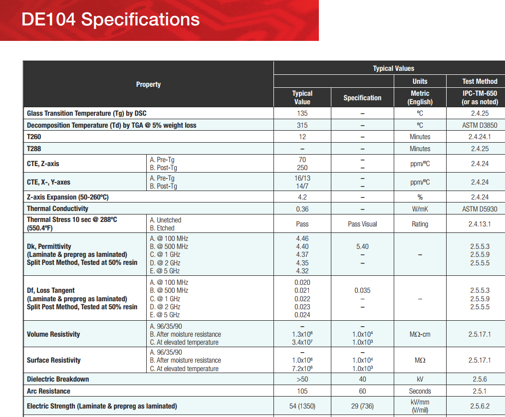
My second question is related to distance d_2 of the sketch above (distances between copper traces of opposing outer layers.) In the datasheet of the Isola Duraver DE104 FR-4 material a dielectric strength of 29 kV/mm is specified:

Datasheet FR-4

Given the standard thickness of 1.55, a maximum voltage of 44.95 kV could be sustained, am I right?

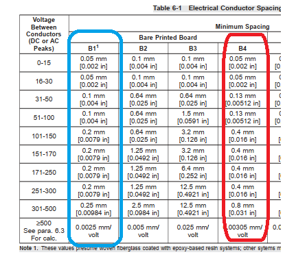
If my computations are correct, then why does IPC-2221 require a much wider spacing between conductors? (B1 is for internal conductors and B4 are external coated conductors.)

IPC-2221

Are they taking into account worse materials, or is it because of safety margins?

\$\endgroup\$
7
  • \$\begingroup\$ Top surface will be subjected to pollution. Inner ones do not. Will you apply high voltage continuously or just a quick test? \$\endgroup\$
    – winny
    Commented Jan 18 at 11:55
  • \$\begingroup\$ MEC does not consider soldermask as insulation, regardless of published material properties. If your board manufacturer can guarantee soldermask thickness then you could probably up-rate a bit but I would build in a design factor of at least 2. \$\endgroup\$
    – vir
    Commented Jan 18 at 12:07
  • \$\begingroup\$ @winny Voltage will be continuously applied. Solder mask should provide protection against pollution \$\endgroup\$
    – Ken Grimes
    Commented Jan 18 at 12:38
  • 2
    \$\begingroup\$ If continuous, the dielectric breakdown is not to be designed for as it's the very short impulse voltage it can withstand. You will have partial discharge, electro migration and/or tracking before that if applied continuously. At 16 kV, I would apply well over 100 mm spacing, depending on CTI of the PCB. \$\endgroup\$
    – winny
    Commented Jan 18 at 12:55
  • 1
    \$\begingroup\$ Do not depend on soldermask for insulation, that is not its purpose. Same with conformal coating. Do you have any connections to the board? How are they insulated? Do you understand that you must avoid sharp points at these voltages because they can create local high electric fields? \$\endgroup\$
    – Mattman944
    Commented Jan 18 at 14:15

2 Answers 2

1
\$\begingroup\$

Creepage will reduce dielectric strength over time.

And creepage will proceed along the easiest trace, not necessarily the direct line. In your example, this is either along the board/resist interface with its undefined properties, or through thin parts of the resist and along the top surface.

The distance rules are there to provide safety margins despite these creepage effects.

\$\endgroup\$
1
\$\begingroup\$

Soldermask, if applied solidly as an approved insulating coating, has excellent dielectric rating, as you can see.

This is rarely the case in practice, however. Soldermask is applied as a liquid, prone to pinholes, bubbles, and variable thickness as surface tension pulls it over the uneven surface of traces; as well as printing errors, handling blemishes, and it can flake off due to handling or perhaps soldering too, particularly the weaker grades popular among proto fab services.

Therefore, for almost all cases with standard fab, the insulation between traces must be treated as air, plus creepage along the board surface. See safety regulations/standards such as IEC 62368-1.

If you need high insulation rating, consider a custom build -- ask your PCB fabricator or assembler for an approved coating process, whether soldermask based, conformal coating, or partial potting compound, or consider potting the thing whole in an enclosure (use vacuum to prevent voids!).

Or, similarly: the PCB material itself may count as a cemented joint. The ratings between layers, and between traces on inner layers, can be considerably higher than on the surface. Mind that the current rating tends to be lower (traces are surrounded by thermal insulation too), and the voltage rating depends on approvals -- I've seen materials that are not rated as a "cemented joint" on inner layers, and therefore must be designed with creepage and clearance still in mind!

\$\endgroup\$

Your Answer

By clicking “Post Your Answer”, you agree to our terms of service and acknowledge you have read our privacy policy.

Not the answer you're looking for? Browse other questions tagged or ask your own question.