0
\$\begingroup\$

I want to make a small flyback HV generator:
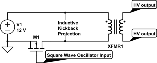
schematic

simulate this circuit – Schematic created using CircuitLab

First of all please forgive me for any stupid mistakes, I am a noob in circuit design.

The MOSFET turns on or off, letting current flow intermittently through the transformer, but when it switches off, the transformer primary's inductance generates a high voltage spike attempting to continue to push current through the open circuit, damaging the MOSFET. I cannot use a regular flyback diode as it will defeat the whole point of the "flyback" action of the transformer; so in other words, I want to allow the kickback to a point, say 50% of the maximum voltage of the MOSFET. I could use an RC snubber, but it is somewhat inflexible if I want to experiment with the input voltage, frequency, etc. I could use 2 back-to-back zener diodes, or I could use a TVS diode. I am not sure the zeners will like those rapid discharge pulses, though, as they are meant for continuous operation. TVS, or transient-voltage-supression diodes are meant for suppressing ESD and such, and although Diotec seems confident that their 1.5KE TVS diodes are suitable for "free-wheeling diode" applications, and it also has a "steady-state power dissipation" value on their datasheet. However, I am cautious. Could anyone provide some guidance?

EDIT: here is the datasheet for Diotec's TVS diodes: https://diotec.com/request/datasheet/15ke68.pdf

EDIT 2: I have edited the schematic following Tim Williams's suggestions

\$\endgroup\$

2 Answers 2

1
\$\begingroup\$

There is a problem... well, two problems probably:

  1. You show a square wave applied to a source follower. This could be done, but is generally more trouble than it's worth. Since your load is isolated (a transformer), it should be trivial to rearrange to something more convenient. Normally we tie source to GND, and then the gate drive circuit can be common-ground with it; the load (primary) goes in the +V to drain path.
  2. Your circuit has no ground indicated, so, it's not even obvious what the square wave would even be applied relative to. Most would assume the supply negative would be ground.

Note that the supply itself may have inductance. Mere wiring length is enough: stray inductance accumulates to the tune of 1μH per meter of length. Even short leads from, say, a lead acid or Li ion battery, or power supply, can stack up a few 100 nH, and this can generate some 10s of V at typical power-switching currents and speeds (V = L dI/dt, for example say L = 100nH, dI = 10A, dt = 100ns). It is a good plan to have a local bypass capacitor (say, 1000s μF electrolytic), and by "local" I mean within mere cm of the transistor, diode(s), and winding terminals. Keep that loop small, and the transistor will stay happy.

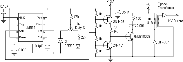
You may find this of interest as a starting point for further testing:

enter image description here

Source: my website, Electronic Circuits 2008-2010, High_Voltage_Supply.png

With the drive circuit as shown, MJE18008 can be trivially replaced with a MOSFET, and then the UF4007 isn't relevant. Instead of the 100Ω + 0.001μF RC snubber, an RCD or TVS clamp snubber can be used (TVS is easiest applied in the UF4007 position).

HV switching BJTs like MJE18008 aren't actually bad in a circuit like this, if one is using the original primary winding on the flyback (typical CRT sets used a 100-200V supply for deflection and video amps), of course then +V needs to be comparable. For a small/added winding (like the "10T" shown), a 12V supply and 200V+ MOSFET might be fine.

If you don't mind the power dissipation, older MOSFET types may prove more robust. Newer types tend not to handle avalanche breakdown very well, but older ones (such as IRFxxx family) often handle it repetitively, limited only by power dissipation.

Note that most driver circuits (including the above) do not make any constraint on switch voltage or current, so will happily explode as many transistors as you overload with them.

Note also, obviously for any high voltage project, lethal voltages are involved, and lethal currents are easily stored up (DC-output flyback transformers have internal capacitance, and accumulate charge on anything they're pointed at!). If a high voltage source ("high" in the sense of, beyond SELV) is powering it (like for using the internal primary winding mentioned above), safety extends to that as well -- more things to keep in mind, more things to potentially go wrong. Only operate on deenergized circuits, and check that capacitors and outputs have discharged before touching them.

\$\endgroup\$
-1
\$\begingroup\$

Neither. You need a rectifier diode, designed to conduct half of the time.

I cannot use a regular flyback diode as it will defeat the whole point of the "flyback" action of the transformer

What? no. You need to clamp, one way or another to burn the leakage energy, and a Zener is generally a method, but might not be up to high currents when needed.

You'd often find clamping circuits that emulate an idealized diode with a knee somewhere at the desirable voltage.

But the standard way is really an R-C diode snubber, with a standard rectifier diode.

\$\endgroup\$
4
  • \$\begingroup\$ Can you please explain? Doesn't the high voltage output of the flyback transformer (more than you'd get if you drove it with a sine wave) happen because of the high voltage induced in the primary when it switches off? Sorry it is probably a very stupid question... \$\endgroup\$ Commented Jul 29 at 17:06
  • \$\begingroup\$ it's not! The stored energy is generally transported to the secondary side; that's how the flyback supply works, after all. What you do get is the inductive kickback from the transformer leakage, and you classically try to store that current in the snubber capacitor, through the diode. \$\endgroup\$ Commented Jul 29 at 17:11
  • \$\begingroup\$ A lone rectifier diode would destroy most or all of the high voltage output. A zener in series with a rectifier, or a zener across the transistor, absorbs excess energy without reducing secondary voltage nearly as much. "Zener" and "TVS" (of the generic/unqualified zener/avalanche diode type) are identical as far as I know, with manufacturer-approved applications (i.e. peak ratings) being the only differentiator. \$\endgroup\$ Commented Jul 29 at 17:44
  • \$\begingroup\$ (RCD peak clamp snubber is fine, it just needs to be dimensioned for maximum output, since the clamp voltage varies with power level.) \$\endgroup\$ Commented Jul 29 at 17:45

Your Answer

By clicking “Post Your Answer”, you agree to our terms of service and acknowledge you have read our privacy policy.

Not the answer you're looking for? Browse other questions tagged or ask your own question.