As a general rule: avoid superstitious practices that aren't justified with cold, hard data.
Even then, the data must be read and understood carefully, to draw conclusions about it; to parse it into effective circuits for example, to relate dimensions of, say, some particular layout (e.g. trace length, via spacing, ground plane size, etc. etc.), are playing what role in that effective circuit. Ultimately, we would like to generalize such data into practical rules and means of calculation, but this is not a straightforward process, and subtle but important features are often susceptible to oversight.
The guard ring concept in particular, strikes me as a superstitious practice inferred from DC/galvanic/low frequency analysis and inappropriately generalized to the wideband frequencies of ESD. In particular, the idea that it somehow saves the bulk of the board from direct strike seems silly to me.
I've never heard a guard ring trace suggested for EMI purposes, but I have heard it in regards to ESD, so I will concentrate on that.
ESD Analysis
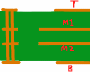
Consider a cross-section around the perimeter such as so:

where T and B are outer copper with whatever (signals etc.), and mid layers are planes. Or for 2-layer, the outer layers are poured and stitched, and signals are kept away from the edge.
The geometry is a shorted-stub transmission line (an asymmetrical edge-coupled coplanar geometry, with one side being a wide ground plane), wrapped around the board. It therefore has all the frequency response of a TL stub, and both resonates at characteristic frequencies, and transmits the ESD surge promptly around all edges of the board itself, whether you meant to have ESD+ringing there or not.
Put another way: instead of the tip of an ESD gun looming over the edge of the PCB, you've got an ESD gun and the several inches of guard ring that become energized in the glorious nanosecond or two immediately following the spark discharge. You're applying more electric field to nearby components, and that just doesn't sound like a winning move to me.
Furthermore, the TL and isolation gap necessarily waste board area, which could otherwise be spent on solid ground plane. Ground plane is an effective conductor / shunt / shield, carrying ESD along and around the board -- along the edge, away from circuitry within. By all means, keep components and signal traces (and supply traces lacking bypass caps) away from the edge, enforced with other-net and mechanical keepouts if necessary, but by all means fill that area up with solid metal to the fullest extent suitable in the design.
Or even clearance entirely -- perhaps you can just not get touched by ESD, by pulling copper in from the edges far enough that a strike doesn't hit. This isn't going to be meaningful/effective on a standalone board, but a board in a plastic enclosure could win enough clearance from seams in the enclosure that a spark can't find a path to it from the outside.
But this, too, is just my opinion -- an informed one perhaps, but I don't have test data to support my claim.
Diversion: On Knowledge
Keep in mind that ESD testing isn't a high-information process. Results obviously depend critically on what the circuit actually is -- some are more sensitive than others, some pick up interference, some are garbled momentarily from the surge, some latch up entirely, or are destroyed by a direct hit. But results are also inconsistent between hits, as an ESD pulse might coincide with some phase of a repetitive signal, or the start, middle or end of a communication frame, or the gap inbetween; and devices may accumulate wear from absorbing surges, and fail after some random number of hits, or erratically over time once partially damaged.
It is not enough to say "we put a guard ring on the board, hit it with ESD, and it seemed to work" -- very likely the circuit would've worked anyway. Conversely, a failing circuit likely fails by a steep enough margin that it's going to fail regardless.
When one is able to do ESD testing with a variable source voltage, and is able to measure accurately the amplitude affecting the circuit itself, there is high information available: the frequency response and gain of the ESD strike - guard ring (if applicable) - circuit system. But it's rare that this happens, and it's not easy to arrange: measuring ESD differentially within a given circuit, without embedding that circuit in a massive ground plane (that would, by its very nature and presence, change the results anyway!), is highly nontrivial -- even very fast, high-CMR(R) differential probes struggle to probe a scenario like this. ESD has significant energy at 300MHz and beyond.
Only in this last sense, can we meaningfully measure the effect of a guard ring. It's still not a good measure, because we have structural tradeoffs (it could be solid ground instead, or completely blank) that we can't express in terms of dB and frequency response or waveform. Ultimately, our only recourse is to test the specific system in question; or perhaps do board-level simulations ($$$) to, effectively, virtually probe it without the complications brought by real probes.
Regarding EMI
It won't do very much.
Fields at the edge of the board simply flow around the trace, and in part, couple into all the resonant modes of the ring, where the whole perimeter potentially becomes a multi-mode antenna. Maybe the coupling is low, but the thing is, coupling from the board edge to open space will be low anyway. It's like trying to block a fan with a mesh screen: most just flows on by unimpeded.
The question didn't state whether something could/should be connected to the guard ring or not. My basic reading of it (and likely casual viewers' too) is a separate trace or other metal looping around the board.
Certainly, a shield can could be attached here: but this simply reduces to the case of a metal enclosure, with all its advantages, and requirements. In particular, it seems to be worse than shielding to the board ground proper, as cables' common mode voltage will not be referenced to the shield, but to some arbitrary point within the board. Fields within and around the board itself will couple into the shield, changing the board's potential by reaction, and thus radiating up any cables leading away from the board.
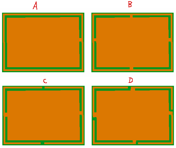
I'm also assuming that "guard ring" refers to just that, a ring, isolated from the board around most of its perimeter, either terminated with one ground return (A), or completely isolated (top view):

Or perhaps several grounds (B); analogous scenarios might include split structures, like a trace open at one or both ends (D), and grounded at the other end, or somewhere in the middle (C).
This is different from the case of simply bringing ground up to the board edge, which I've recommended above, and is generally recommended elsewhere.
(The article in question even notes that ground can be brought to the edge: but by seeming to include this under the same umbrella, they commit the sin of ambiguating the term "guard ring". For purposes of this answer, I am ignoring that assertion, and assuming the geometry of the question's first image as example.)
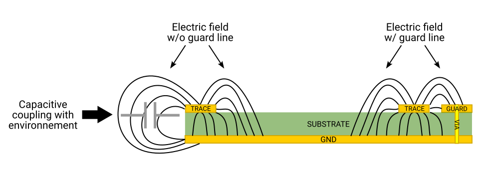
That is, in contrast to this geometry all around:

The ground plane extended laterally and then vertically, wrapping around the board edge, actually terminates field lines.
Thus, I don't see any value in the "ring" practice, whether mostly or entirely separated, segmented, or shielded. If you need good shielding, simple extend the reference plane of the circuit. Nothing more to it than that.
Ground To The Edge
This is related -- but distinct from how I understand the question. So, consider this a "no, but..", or a "perhaps you meant--?", or better still, a "if you must, do it this way".
So, going on from the idea of extending ground to the edges. Consider the case of a multilayer board, where inner power plane is used:
There can be some noise between planes, and the board edge serves as an open-waveguide antenna structure, coupling that noise to free space. Why you're allowing such frequencies and magnitudes into the plane, is a good question by itself, but in the event that such happens, it can be useful to pull back the plane from the edge, and extend ground. Diagrams here:
Why Some PCBs Need Edge Plating? | PCBWay
Although this article isn't very in-depth, it does hit the basics, and to my surprise, even includes some references for further reading. And there's always Ott's Electromagnetic Compatibility Engineering, and a few other prominent and reasonably comprehensive texts that are excellent reading.

