0
\$\begingroup\$

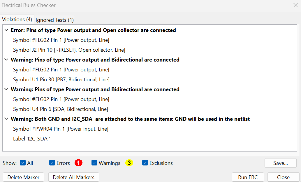
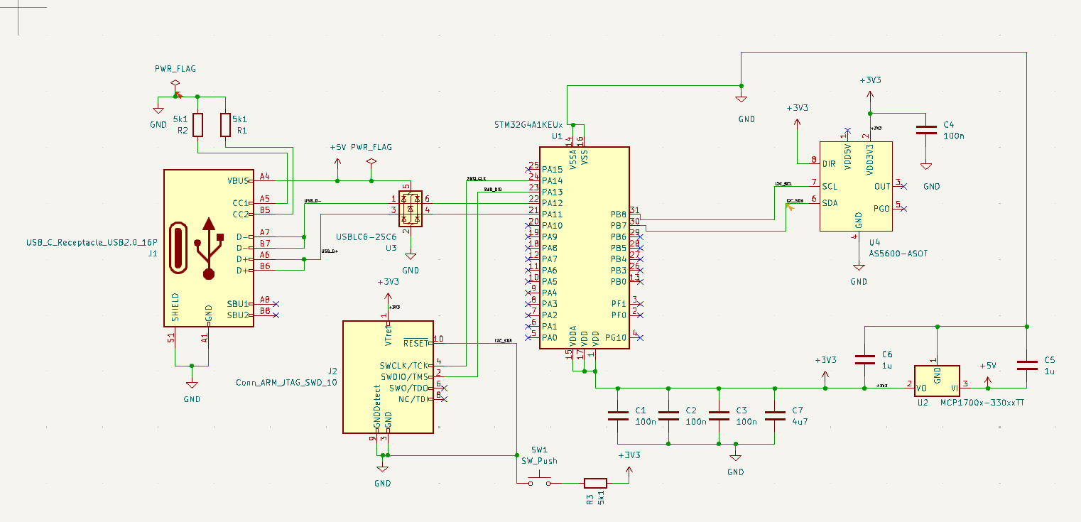
For a project in my studies, I need to design a schematic for a PCB. I've already created the following schematic, which you can see in the attached image. However, I’m still getting one error and three warnings, and I’m not sure how to resolve them.

Image of my schematic Image of the erors List of parts I habe to use

\$\endgroup\$
3
  • \$\begingroup\$ General comment to the schematic - its OK that you flipped the symbol for U1 to get the lines to not cross on U3 and U4. That's more or less tidy. You should not wire GND and VDD the way it is wired, though. Higher potential goes on the top, and lower on the bottom. Input->output-flow is left to right. U2 should not be rotated 180 degrees, and the GND-wire should not be combined with the one from U1. \$\endgroup\$
    – MrGerber
    Commented Oct 6 at 12:56
  • \$\begingroup\$ U2 should be with VI facing left, in the top left of the schematic, with GND power symbols for itself, surrounded by it's capacitors, a +5V flag and a +3V3-flag. U1 should have it's VDD pins connected to one +3V3-flag (pointing up as you have it now), and the VSS and VSSA-pins connected to a GND-flag (pointing down like you have it now). \$\endgroup\$
    – MrGerber
    Commented Oct 6 at 13:00
  • \$\begingroup\$ My personal preference is to have the decoupling caps connected with their own VDD and GND-flags, grouped as they would be grouped in the layout, and with a note on the schematic telling to keep them close to their respective pins, but some people do it the way you have done it already, having all of them wired to the VDD-pins directly. \$\endgroup\$
    – MrGerber
    Commented Oct 6 at 13:01

1 Answer 1

0
\$\begingroup\$
v Error: Pins of type Power output and Open collector are connected
  Symbol #FLG02 Pin 1 [Power output, Line]
  Symbol J2 Pin 10 [~{RESET}, Open collector, Line]
v Warning: Pins of type Power output and Bidirectional are connected
  Symbol #FLG02 Pin 1 [Power output, Line]
  Symbol U1 Pin 30 [PB7, Bidirectional, Line]
v Warning: Pins of type Power output and Bidirectional are connected
  Symbol #FLG02 Pin 1 [Power output, Line]
  Symbol U4 Pin 6 [SDA, Bidirectional, Line]
v Warning: Both GND and 12C SDA are attached to the same items; GND will be used in the netlist
  Symbol #PWR04 Pin 1 [Power input, Line]
  Label '12C_SDA '

Error 1 "Pins of type Power output and Open collector are connected"

Open collector connected to power output: An open collector pin is a pin that can only pull what it is connected to, down.1 That is why KiCAD is throwing an error. Your /RESET line on the SWD connector is not connected to anything but the GND-pin. It should not be connected to GND, (that would hold the MCU in reset forever) but to the NRST pin on the STM32G4A1 - PG10 - Pin 42. This has a weak pull up inside the chip.

.

Warnings 1-3 "'Pins of type Power output and Bidirectional are connected' and 'Both GND and 12C SDA are attached to the same items; GND will be used in the netlist'"

All three warnings are related to the same problem but is reporting it in three different ways.

The connection between pin PB7 on U1 and the SDA pin on U4 has the I2C_SDA label on it, which has also in some way duplicated itself on to the /RESET line on pin 10 on J2. Remove the I2C_SDA label from the /RESET line, and all three warnings should go away. enter image description here
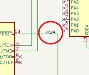
The first two warnings are related to IO lines being connected to a power output pin - one report for U1 Pin 30 (one end of I2C SDA) and one report for U4 Pin 6 (the other end of I2C SDA) being connected to GND because of the misplaced label.

The final warning is the one that tells you that you have misplaced that SDA label - it's saying "you have one connection you have given two different names - GND and I2C_SDA", and that it will prioritize GND.

1 Read more in this question about open collectors

2 STM32G4A1 datasheet
\$\endgroup\$
2
  • \$\begingroup\$ Thank you for your help, it was very helpful! \$\endgroup\$
    – Big 1234
    Commented Oct 6 at 14:43
  • \$\begingroup\$ If the answer was helpful it is good practice to upvote, and if it solved your problem, please mark as "accepted". See What should I do when someone answers my question? \$\endgroup\$
    – MrGerber
    Commented Oct 6 at 15:38

Your Answer

By clicking “Post Your Answer”, you agree to our terms of service and acknowledge you have read our privacy policy.

Not the answer you're looking for? Browse other questions tagged or ask your own question.