20
\$\begingroup\$

It seems like there has been so much research being done on making circuits and components that are smaller and smaller, but at a certain point we are going to be designing components and boards that are literally just a few atoms wide.

Why is it that companies pour so much money into making say a 4 layer circuit board that is 10 square inches still only a flat 4 layers but maybe 8 square inches, rather than just making an 8 layer board only 5 square inches for example? (8 is still possible and it is done, but why isn't this taken up to say 100 layers or more?)

Also does this same principle apply to IC design? Are ICs usually only a few layers and spread into thin sheets, or are they typically built more vertically?

*Edit: So one thing that has become apparent to me from the comments is the fact that in circuit board design you can only really place components on the outer 2 layers. That would make inner layers unnecessary for anything other than weaving. What about in IC design, something like an intel processor? Are there still special components on the outer two layers, or is a processor more 3D than a circuit board?

\$\endgroup\$
13
  • 4
    \$\begingroup\$ One word: price. \$\endgroup\$
    – winny
    Commented Jul 16, 2017 at 0:03
  • 29
    \$\begingroup\$ Most PC motherboards now are 8, 16 or even 32 layers. \$\endgroup\$ Commented Jul 16, 2017 at 0:10
  • 1
    \$\begingroup\$ One radio module that I work with is built on a 12 layer circuit board. Very expensive module but it works better than anything else that I've used to date. \$\endgroup\$ Commented Jul 16, 2017 at 2:15
  • 8
    \$\begingroup\$ Why do you think that boards with such high layer counts are not being made for specialized applications? \$\endgroup\$ Commented Jul 16, 2017 at 4:15
  • 1
    \$\begingroup\$ In ICs there are usually upwards of 50 layers to work in. Metal layers, polysilicon layers, doping layers (n and p at different depths) front side backside etc. Only a few of there are 'active' layers. ICs are fairly 2D in terms of components, but the components are made from many layers, so 3D in that sense. You could not put two transistors one 'on top' of the other in most standard IC processes because they will use many of the same layers in their construction. \$\endgroup\$
    – IC_Eng
    Commented Jul 17, 2017 at 14:46

9 Answers 9

50
\$\begingroup\$

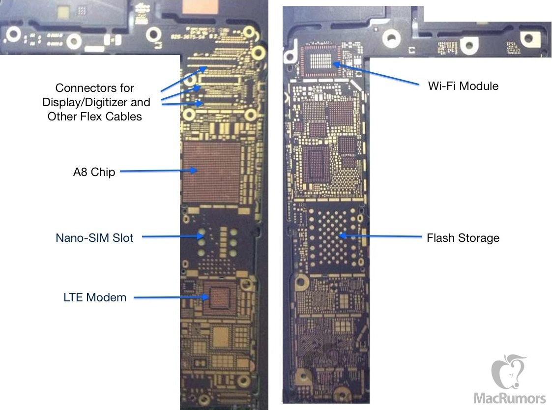
Let's have a look at this iPhone PCB.

enter image description here

Notice there are no traces, only pads with devices stuffed right next to each other everywhere on both sides.

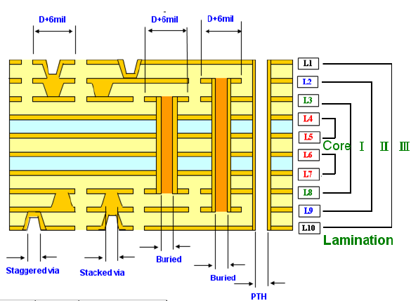
This is HDI (High Density Interconnect).enter image description here

This is very neat. Basically you pay extra to have the 1-2 outer layers on one or both sides etched with extremely tiny features. The inner layers, which are mostly power and ground planes anyway, are etched using regular cheap processes.

Tiny microvias are laser-drilled into the pads to connect the surface to the next high density layer. There also blind and buried vias.

Simplifying things... the main problem with standard PCBs is vias. They go through the whole board and eat up space on all layers. You can add layers if you want, but they'll still be full of holes! And it gets expensive. You can't shrink a via hole below the size of the drill, and the drill has to be tough enough to actually... you know, drill the whole board without breaking... so it can't be too small. Also, everything has to align and register properly. Precision stuff is not cheap.

However, a microvia only goes through one or two very thin layers, so it can be drilled with a laser, and the hole can be much smaller. These, and also Blind/Buried vias free up space on other layers and allow to route more traces, and put components on both sides.

Each layer can do a lot more with these technologies.

\$\endgroup\$
1
  • 6
    \$\begingroup\$ PS: Laser ablates material by superheating it, essentially it makes things go poof. You don't want that to happen at the bottom of a very narrow hole, expanding gases in confined spaces and all that... \$\endgroup\$
    – bobflux
    Commented Jul 16, 2017 at 11:54
26
\$\begingroup\$

I don't know which boards you're looking at, but high layer counts are definitely used where it makes economic sense. Have you looked at the motherboard of a PC or cellphone lately? I regularly work on compact special-purpose products that have anywhere from 6 to 12 layer PCBs. In particular, high pin count BGA packages require a certain number of layers just to make the connections (a.k.a. "fanout") to the inner balls.

But part of your question doesn't make sense. You can't in general replace a 10 sq. in. board that has four layers with a 5 sq. in. board that has 8 layers — it doesn't work like that. Remember, components can only be mounted on the outer two layers, which puts a lower limit on the area of the PCB. Connections between those components and the inner-layer wiring require vias that also take up area on the outer layers. Blind and buried vias can somewhat mitigate the amount of area required for wiring, but they add additional processing steps and cost to the board, too.

In many cases, the size of the board is dictated less by the number of components and more by the placement of external connectors, etc. that makes the most sense from a packaging (and user experience) point of view. For example, using a single "oversize" PCB that stretches all the way from the front to the rear of the box may make sense if it eliminates the expense of making two separate assemblies with cabling between them. Then the designer has the "luxury" of spreading the components out a bit and using fewer layers. The final BOM cost is often lowest using this approach.


Responding to your edit about IC design: Actually, ICs have only ONE layer of active components, which is even more restrictive than a 2-sided PCB. However, the minimum feature size of the active layer is typically much smaller than that of the metal wiring layers above, so there's considerable benefit to having multiple wiring layers.

The limiting factor becomes the fact that the vias from any wiring layer to the active layer must go through all of the lower wiring layers, limiting how much wiring can actually be done on those lower layers. Therefore, the lowest layers tend to be used for the "most local" connections only, and the higher layers for the more far-reaching connections and global connections such as power supplies and clock signals.

\$\endgroup\$
24
\$\begingroup\$

As a Printed Circuit Board designer, I can say that it is all down to cost. I have designed boards up to 56 layers, but this was a very specific case were cost was not as much as an issue as performance. One other limitation is board thickness; the laminates used can only be so thin, and when you add all the layers to over 14-16 layers, the board thickness starts to exceed the standard of 1.6mm, and in the case of that 56 layer board I designed the thickness was over 5mm. If you were to use through hole components, you come across the issue that these parts have pin lengths designed to fit a board with thicknesses not greater than 2mm, and if you exceed that you won't have enough pin to solder to, therefore failing to pass the IPC standards for assembly quality. The alternative would be to select the parts that have longer pin lengths (not many) or have them custom made ($$$).

When it comes to IC design, the layer concept is slightly different as the manufacturing happens mostly by deposition, but in the same way as it is for the PCBs, each layer adds time to make, and therefore cost.

\$\endgroup\$
3
  • 14
    \$\begingroup\$ +1 If I may ask, what was the 56 layer board for? (Just curious.) \$\endgroup\$ Commented Jul 17, 2017 at 14:45
  • 1
    \$\begingroup\$ @HaLailahHaZeh The highest layer board I've seen was over 40 layers, and held 12 of the (at the time) highest gate count FPGAs for use in scientific computing. Huge chips with hundreds of BGA pins that all had to connect to each other and the connectors on the PCB. The PCB Guru may not be able to discuss their project further than they already have, but you can guess that the project was specialized, low volume, high budget, and had thousands of nets to route between some very large chips, probably involving FPGAs or ASICs beside some more common chips. \$\endgroup\$
    – Adam Davis
    Commented Jul 18, 2017 at 13:00
  • 4
    \$\begingroup\$ @HaLailahHaZeh, I worked for a few years designing boards for ATE (Automatic Testing Equipment), and more specifically, designing boards that would be the interface between the ATE and the semiconductor that needed to be tested. In this case the board was to test a Mainframe processor which was a BGA with 3800+ balls. The reason for having that many layers was that the power consumption of this device was massive, and required multiple 2oz copper on the inner layers to resist to current peaks of 300A on each power branch. the rest was GND and 15 or so signal layers. \$\endgroup\$ Commented Jul 22, 2017 at 12:02
15
\$\begingroup\$

We do. PCB's go 16 layers thick if not much thicker.

IC's are one layer of transistors and then 16-32 layers of wires on top.
2.5-d IC's are stacks of these on top of eachother with interconnects between the silicon wafers.
3-d IC's would actually have multiple layers of transistors, but I'm not sure there's many manufacturers doing that.

The main reason for trying to keep layers to a minimum is simply cost. Every penny costs when you're manufacturing a lot of something. More layers = more time and more cost. When you need the layers you need them though and they're there for you if you've got the green.

\$\endgroup\$
2
  • 1
    \$\begingroup\$ Does 3d flash count? It uses columns of up to 64 cells to increase density, but I'm not sure if anything other than the actual charge traps are in the columns vs on the base layers of the chips. \$\endgroup\$ Commented Jul 17, 2017 at 19:17
  • 2
    \$\begingroup\$ @DanNeely Yup, 3d flash counts as full 3d. According to samsung, they're doing up to 100 layers with their v-nand technology. I would assume they've got control logic on every layer. Otherwise, pumping that much data out would be awful slow. samsung.com/semiconductor/products/flash-storage/v-nand \$\endgroup\$
    – horta
    Commented Jul 17, 2017 at 19:39
5
\$\begingroup\$

Cost reduction is the main reason.

In the mid 80's mainframes, our parent company bought a 200k sqft factory that made 50 layer microgrid tracks in MOBO size and the presses for these boards were massive not to mention the large dumpster sized vats full of liquid gold chemicals for full immersion plating.

WHen I used to purchase PCBs every month for R&D and volume the cost estimates could be reduced to a few lines of specs that basically was the total weight of copper or thickness and area * layers. So adding more layers adds cost unless made thinner. Added costs were outside norm of routing and hole qty and size and under normal 8/8 mil which is down to 3/3mil track and gap now.

The cost to replace a mainframe in performance is like a high end PC that only costs 0.02% of the ownership of a mainframe.

The rule of thumb in the 90's for me was 5 cents per square in on all layers of 1oz Cu

\$\endgroup\$
5
\$\begingroup\$

There is a problem 2 layers (with PTH) solve: Traces cannot cross without taking advantage of some component (or bridge/zero-ohm/...) crossing it.

There is a problem 3 layers solve: Ground returns for low-level or high-frequency signal traces are on a different route than the trace itself, causing ground loops, undefined trace impedance, inductive coupling, and bad shielding. A ground plane is more or less equivalent to an exactly parallel ground return trace (since it forms the lowest-inductance loop).

There is a problem 4 layers solve: Power distribution wiring takes space from signal traces and adds complexity.

There is a problem 5 layers solve: Low level or RF analog circuitry and digital (pulse) and/or power circuits share a ground, and the slightest ground shift caused by the latter gets heavily amplified by the former.

Anything beyond that is just catering to additional complexity and/or extra power rails...

\$\endgroup\$
4
\$\begingroup\$

The thinnest PCB pre-preg that is made corresponds to around 2 mils per layer so more than about 30-32 layers (and no core) is going to require a thicker board than the usual 1.6mm.

The cost per cm^2 of a 14 layer board vs. 4 layer board is about 5-6:1 in quantity 100 and 12:1 in quantity 10, in other words the setup costs are quite high as well as the variable costs.

You can only get the parts so close together so the savings are real, but limited, with higher layer counts. Savings are also achieved by using the smallest possible packages such as BGA or chip scale packages and the smallest passive parts (smaller than 0201), using very fine lines (3 or 4 mil, for example), using blind vias, buried vias, microvias, and leaving out designator printing. Each of those things cost more and require a higher level of technology for the same level of reliability.

In general high layer count boards cost more for the same connectivity (performance may be better with more ground planes, so I don't say equivalent functionality) and have much higher fixed costs so are less likely to be seen in low volume or cheap devices.

A smartphone is an example where the cost is justified, but most products don't need (or can't afford) to use the very smallest IC and other packages crammed as tightly as possible together.

ICs, as I understand it, may use many (tens) of layers of metal for connectivity (complex digital ICs such as CPUs which may have over a billion transistors, not simple analog chips).

\$\endgroup\$
3
\$\begingroup\$

There are many factors that determine layer count:

1. Power distrubution.

It is not unusual to see 6 or more power rails on a moderately complex board. Proper distribution can be quite a challenge (particularly if there are high speed links such as PCI Express, Fibre channel 4x or even 10x, Infiniband, 10G ethernet, SMPTE292 or faster).

The power requirements alone may need multiple layers; a director class Infiniband switch I designed 14 years ago had 1.2V @ 100A on the switch node boards. A high brightness LED to drive a head up display took 15A at ~4.5V. These types of requirement push for multiple power and ground layers alone. 8 layers for power is not uncommon in such cases.

2. High density layout.

Apart from layer count, vias are a cost driver; it can be less expensive to add a couple of layers if via count can be reduced. Via hole size also drives cost; although the ordinary minimun hole size of 0.3mm will not normally add much cost, exceeding the aspect ratio of board thickness to via drill size of 8:1 definitely will because the fabricator knows this will drastically increase drill bit breakage. This is a bit chicken and egg as increasing layer count may increase the minimum hole size.

3. Lots of high speed interconnect.

High speed pairs work best with single layer routing (a breakout via at each end only) for a variety of reasons. Consider a PCB with 2 independent DDR3 2100 interconnects, 32 lanes of PCI express at 8Gb/s; all of that demands multiple routing layers. This can be very challenging in a mixed signal (lots of sensitive analog) environment.

Of course we choose the most cost effective layer count, but that is often not the minimum possible, which could introduce reliability issues (pushing the limits on via annular ring size comes to mind.

So the answer is that layer count is determined by application; if we can get away with 4 layers, great. Quite often that is not realistic.

\$\endgroup\$
3
\$\begingroup\$

High layer counts are in fact possible and used in some applications.

But in reality it comes down to cost and reliability.

You need to understand the PCB manufacturing process to really get the true handle on this. The fact is, every layer you add increases the probability that the manufactured stack will not pass functional testing. In particular, interconnections between and through layers can and do fail to connect. As such there are a significant number of scrap boards generated as part of the manufacturing process. The more layers you have increases the manufacturers cost to produce, which, of course, gets passed on to you.

Furthermore, even if it passes testing in manufacture, the probability of those interconnections failing in the field also increases markedly with number of layers.

Sure it would often be easier, especially with todays CAD tools, to just add another layer, but any prudent designer strives to keep the costs down and maximize the PCB itself's reliability by minimizing the layer count. Often that means slight redesigns, clever pin reassignment, changing component types etc.

The decision to add another layer is usually a last resort one.

\$\endgroup\$

Your Answer

By clicking “Post Your Answer”, you agree to our terms of service and acknowledge you have read our privacy policy.

Not the answer you're looking for? Browse other questions tagged or ask your own question.